A petal-type cone-like pattern LED pattern optimized substrate and LED chip

A graphic optimization substrate and petal technology, applied in the direction of electrical components, circuits, semiconductor devices, etc., to achieve the effect of increasing the luminous flux at the bottom

Active Publication Date: 2017-06-06
SOUTH CHINA UNIV OF TECH
View PDF2 Cites 0 Cited by
  • Summary
  • Abstract
  • Description
  • Claims
  • Application Information

AI Technical Summary

Problems solved by technology

Although this can improve the light output rate to a certain extent, with the advancement of technology and the continuous improvement of people's requirements for lighting tools, they can no longer fully meet people's needs.

Method used


Image

  • A petal-type cone-like pattern LED pattern optimized substrate and LED chip
  • A petal-type cone-like pattern LED pattern optimized substrate and LED chip
  • A petal-type cone-like pattern LED pattern optimized substrate and LED chip

Examples


Embodiment 1

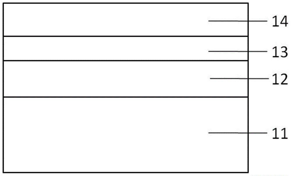
[0027] figure 1 It is a schematic diagram of the LED chip of this embodiment, which consists of a petal-like cone-like LED pattern optimization substrate 11, an N-type GaN layer 12, an MQW quantum well layer 13, and a P-type GaN layer 14 arranged in sequence.

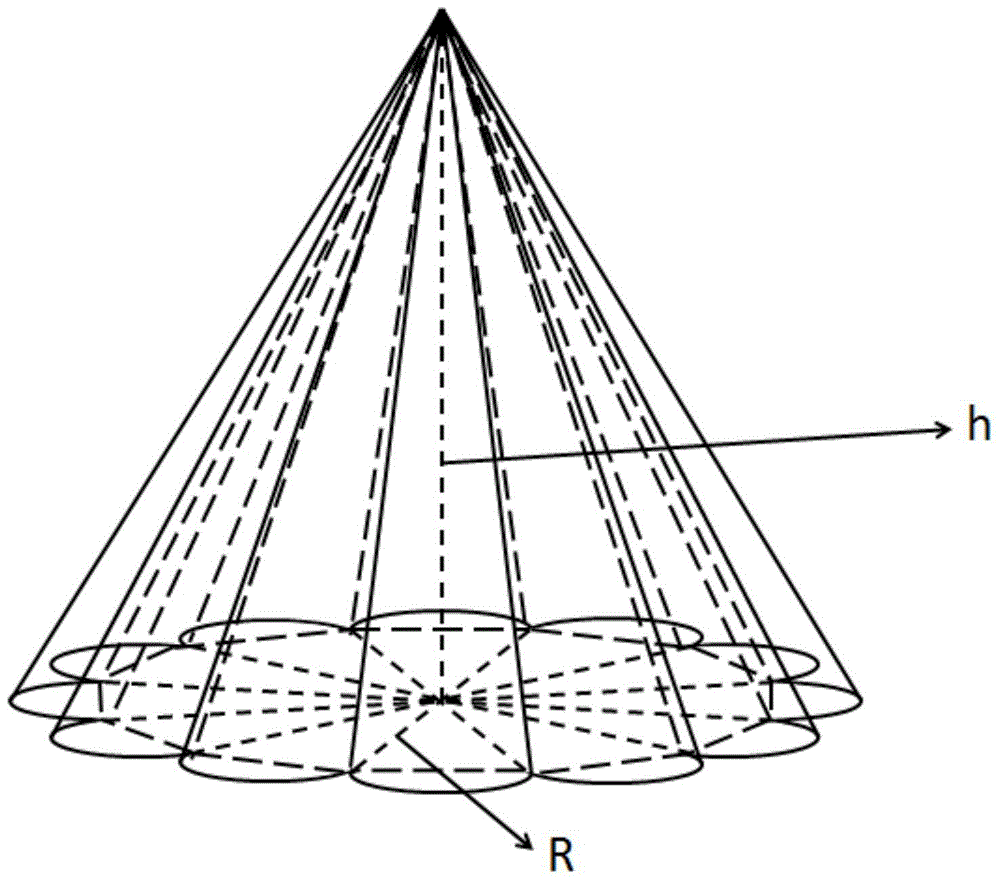
[0028] The substrate pattern is composed of multiple petal-like cones of the same shape arranged on the surface of the substrate; such as figure 2 As shown, any horizontal section of the petal-shaped cone-like body in this embodiment is a petal-shaped figure; the petal-shaped figure is a closed figure formed by connecting 12 circular arcs with the same shape end to end. The distance R between the end point of each arc of the bottom surface of the petal-shaped cone-like body and the center of the bottom surface is 3.0 μm; the height h of the petal-shaped cone-like body is 2 μm.

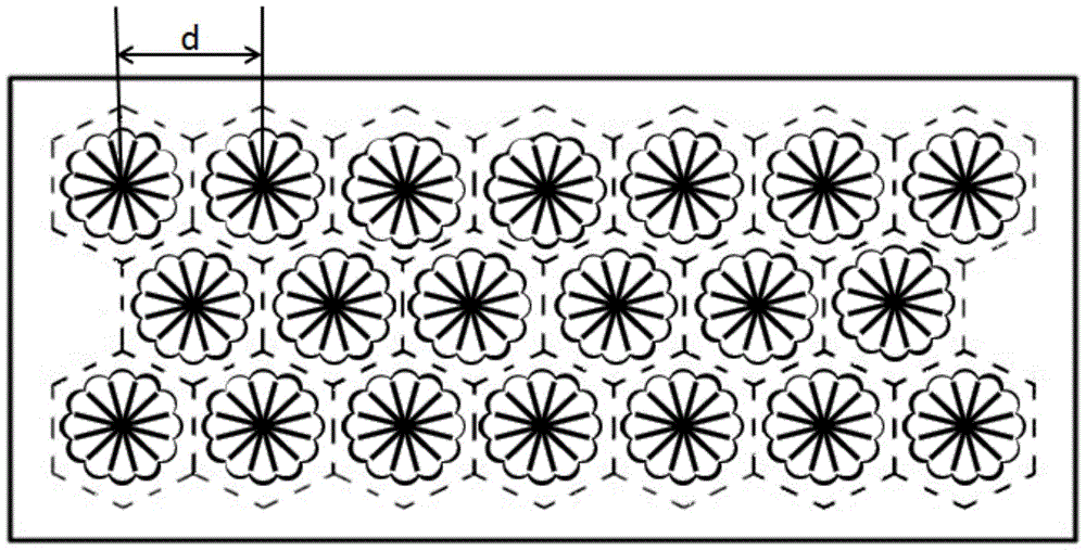
[0029] The same petal-type cones of the present embodiment adopt such as image 3 The hexagonal arrangement shown. The distance d between t...

Embodiment 2

[0031] The LED chip of this embodiment is composed of a petal-shaped cone-like LED pattern-optimized substrate, an N-type GaN layer, an MQW quantum well layer, and a P-type GaN layer arranged in sequence.

[0032] The substrate pattern is made up of a plurality of petal-shaped cones of the same shape arranged on the substrate surface; any horizontal section of the petal-shaped cones in this embodiment is a petal-shaped figure; the petal-shaped figure is composed of 15 A closed figure formed by connecting arcs of the same shape end to end. The distance R between the end point of each arc of the bottom surface of the petal-shaped cone-like body and the center of the bottom surface is 1.7 μm; the height h of the petal-shaped cone-like body is 2 μm.

[0033] The same petal-type cones of the present embodiment adopt such as Figure 4 The rectangular arrangement shown. The distance d between the centers of two adjacent petal-shaped cones is 6 μm.

Embodiment 3

[0035] The LED chip of this embodiment is composed of a petal-shaped cone-like LED pattern-optimized substrate, an N-type GaN layer, an MQW quantum well layer, and a P-type GaN layer arranged in sequence.

[0036] The substrate pattern is made up of a plurality of petal-shaped cones of the same shape arranged on the substrate surface; any horizontal section of the petal-shaped cones in this embodiment is a petal-shaped figure; the petal-shaped figure is composed of 15 A closed figure formed by connecting arcs of the same shape end to end. The distance R between the end point of each arc of the bottom surface of the petal-shaped cone-like body and the center of the bottom surface is 2.3 μm; the height h of the petal-shaped cone-like body is 2 μm.

[0037] The same petal-type cones of the present embodiment adopt such as Figure 5 The rectangular arrangement shown. The distance d between the centers of two adjacent petal-like cones is 6.5 μm.


PUM


Abstract

The invention discloses an LED graphical optimization substrate of a petal type cone pattern, the substrate pattern is composed of a plurality of petal type cones being the same on shape and arranged on the surface of the substrate; any horizontal cross section of the petal type cone is in a shape of petal; the petal-shaped figure is a close figure composed of the arcs being the same on shape and connected together in a head-to-end order connection mode. The LED chip including the LED graphical optimization substrate is disclosed. The LED graphical optimization substrate of the petal type cone pattern increases the refraction reflecting surface and raises the light strength and luminous efficiency.

Description

technical field [0001] The invention relates to an LED pattern substrate, in particular to a petal-shaped cone-like pattern LED pattern optimized substrate and an LED chip. Background technique [0002] At present, in order to improve the internal quantum efficiency and light extraction efficiency of GaN-based LEDs, many new technologies have been applied, including lateral epitaxial growth technology, surface roughening, patterned substrate technology, and metal specular reflection layer technology. In recent years, how to use patterned substrate technology to effectively improve the light extraction efficiency of GaN-based LEDs on sapphire substrates has gradually become a research hotspot in the field of GaN-based LEDs on sapphire substrates. As the key to patterned substrate technology, the substrate pattern has evolved so far, which has significantly improved the LED light extraction effect and epitaxy quality, and has become an important way to improve LED performance....

Claims


Application Information

Patent Timeline
Patent Type & Authority Patents(China)
IPC IPC(8): H01L33/20
CPCH01L33/20
Inventor 李国强林志霆乔田周仕忠王海燕王凯诚钟立义
Owner SOUTH CHINA UNIV OF TECH
Why Eureka
Try Eureka