

LTPS TFT, manufacturing method of LTPS TFT, array substrate and display device
A technology of thin-film transistors and low-temperature polysilicon, which is applied in the direction of transistors, semiconductor/solid-state device manufacturing, semiconductor devices, etc., to avoid and reduce adverse effects
- Summary
- Abstract
- Description
- Claims
- Application Information
AI Technical Summary
Problems solved by technology
Method used
Image

Examples
Embodiment Construction
[0033] The specific implementation manners of the present invention will be further described in detail below in conjunction with the accompanying drawings and embodiments. The following examples are used to illustrate the present invention, but are not intended to limit the scope of the present invention.
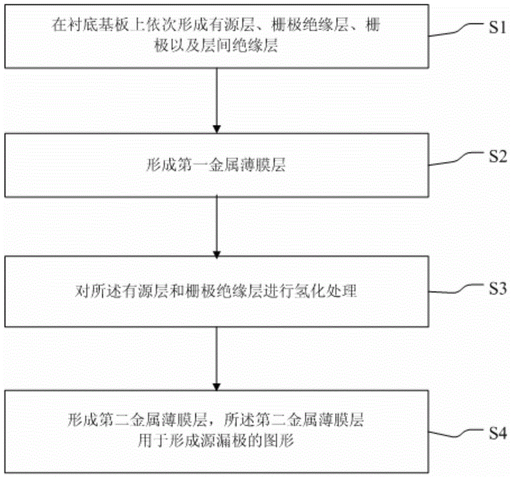
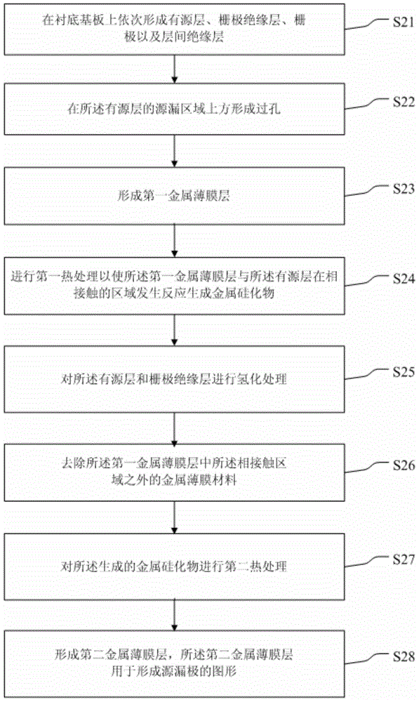
[0034] figure 2 It is a flowchart of a method for manufacturing a low-temperature polysilicon thin film transistor provided in an embodiment of the present invention, including:
[0035] S1: sequentially forming an active layer, a gate insulating layer, a gate and an interlayer insulating layer on the base substrate;
[0036] S2: forming the first metal thin film layer;
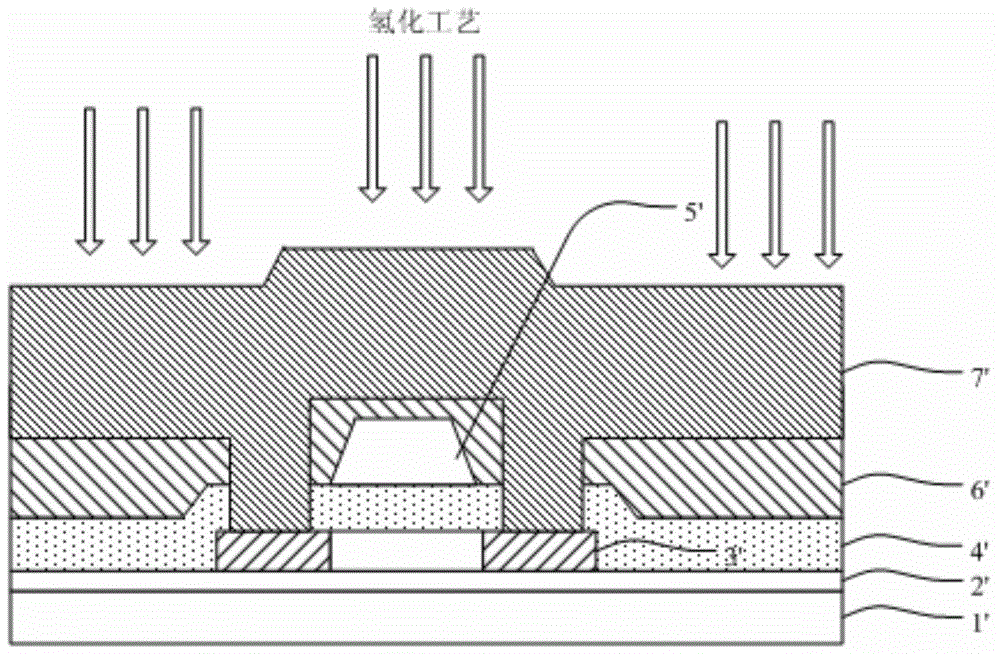
[0037] S3: performing hydrogenation treatment on the active layer and the gate insulating layer;
[0038] S4: forming a second metal thin film layer, the second metal thin film layer is used to form the pattern of source and drain electrodes.
[0039] Wherein, the material of the first metal thin fil...
PUM
 Abstract
Description
Claims
Application Information