A placement machine for bumped wafers

A placement machine and bump technology, which is applied in the direction of electrical components, semiconductor/solid-state device manufacturing, circuits, etc., can solve problems such as fragments, hidden cracks, and hidden dangers left by the process, so as to reduce deformation, reduce edge pressure, The effect of improving productivity

Active Publication Date: 2017-03-29
JIANGYIN CHANGDIAN ADVANCED PACKAGING CO LTD
View PDF5 Cites 0 Cited by
  • Summary
  • Abstract
  • Description
  • Claims
  • Application Information

AI Technical Summary

Problems solved by technology

At the moment when the pressure of the roller is applied to the edge of the bump wafer 100 during placement, due to the existence of the vacancy, it is easy to cause problems such as hidden cracks and fragments on the edge of the bump wafer 100 due to excessive deformation. leave a hidden danger

Method used


Image

  • A placement machine for bumped wafers
  • A placement machine for bumped wafers
  • A placement machine for bumped wafers

Examples


Embodiment 1

[0046] Embodiment one, see Figure 2 to Figure 4

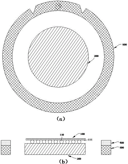
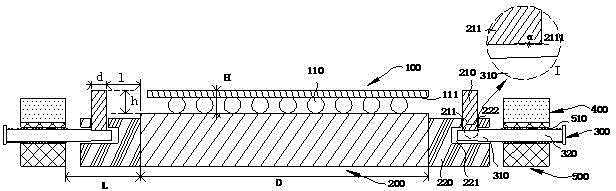
[0047] A kind of placement machine for bump wafer of the present invention, as figure 2 and image 3 As shown, the bump wafer 100 to be mounted is carried on the mount chassis 200, and the bump wafer 100 is temporarily fixed by vacuum suction to facilitate the mount. Wherein, the thickness of the bump wafer 100 and its bump 110 is H. The wafer ring platform 500 is installed around the patch chassis 200, and there is a gap of width L with the patch chassis 200. The side of the wafer ring platform 500 is provided with a threaded through hole 510 pointing to the center of the patch chassis 200. The through holes 510 are evenly distributed, and there are at least three. The wafer ring 400 is also temporarily fixed above the wafer ring platform 500 by vacuum suction.

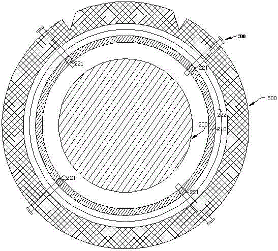
[0048] A dam 210 is set between the patch chassis 200 and the wafer ring platform 500 . The dam 210 is ring-shaped, and the gap between it and the chip chassi...

Embodiment 2

[0053]Embodiment two, see Figure 5

[0054] The structure of this embodiment is similar to that of Embodiment 1, the difference is that: the fixing device 220 is a discontinuous fan-shaped block, and there are at least three, evenly distributed, to simplify the structure, and each fixing device 220 corresponds to a flat head screw 300 . Figure 5 4 fixing devices 220 are shown in , generally only need to adjust three flat head screws 300 among them to meet the requirement of height level.

[0055] When the mounter for bump wafers of the present invention starts filming, as Image 6 As shown, the patch chassis 200 drives the dam 210 to rise together, the patch roller 600 carries the diaphragm and presses down to the bump wafer 100, and then the patch roller 600 rolls from one side of the bump wafer 100 to the bump wafer at a constant speed On the other side of 100, complete the film.


PUM


Abstract

The invention discloses a chip mounter for a bump wafer, and belongs to the technical field of semiconductor packaging. The chip mounter comprises a chip mounting base for bearing the bump wafer to be mounted, a Waferring platform mounted around the chip mounting base, and a coffer dam arranged between the chip mounting base and the Waferring platform, wherein a threaded through hole facing to the center of the chip mounting base is formed in the side surface of the Waferring platform; the height difference between the top of the coffer dam and the top of the chip mounting base is h, and the value of H-h is not less than 0 micron and not more than 50 microns; a boss which extends down is arranged at the lower part of the coffer dam; the coffer dam is connected with the chip mounting base through a fixing device; a blind hole facing to the center of the chip mounting base is formed in the outer side surface of the fixing device; a through hole perpendicular to the blind hole and a flat screw for connecting the through hole with the blind hole are formed over the blind hole, and the tail of the blind hole is matched with the boss. According to the chip mounter, the chip mounting base and the Waferring platform are designed and the coffer dam is added between the chip mounting base and the Waferring platform, so that the problems of easy fragmenting, cracking and the like of edges in a bump wafer mounting process are solved.

Description

technical field [0001] The invention relates to a placement machine for bump wafers, which belongs to the technical field of semiconductor packaging. Background technique [0002] With the development of semiconductor technology, wafers (wafers) tend to become thinner and thinner. Different from the conventional wafer (wafer) with a flat surface, the surface of the bump wafer 100 for processing into a flip-chip (flip chip) is made with raised bumps 110 (bumps or solder balls, solder block), but there is no bump 110 within 3mm of its edge, which forms a vacancy, such as figure 1 shown. At the moment when the pressure of the roller is applied to the edge of the bump wafer 100 during placement, due to the existence of the vacancy, it is easy to cause problems such as hidden cracks and fragments on the edge of the bump wafer 100 due to excessive deformation. Leave a hidden danger. Contents of the invention [0003] As shown above, the purpose of the present invention is to...

Claims


Application Information

Patent Timeline
Patent Type & Authority Patents(China)
IPC IPC(8): H01L21/60
Inventor 孙超罗建忠曾志华李京俊张黎陈锦辉赖志明
Owner JIANGYIN CHANGDIAN ADVANCED PACKAGING CO LTD
Why Eureka
Try Eureka