Transistors and methods of forming them

A technology of transistors and semiconductors, applied in the direction of semiconductor devices, semiconductor/solid-state device manufacturing, electrical components, etc., can solve the problems of unfavorable semiconductor device size reduction, large junction-free transistor size, chip integration, etc., to achieve short channel effect Effects of suppression, device density improvement, and integration improvement

Active Publication Date: 2017-06-16
SEMICON MFG INT (SHANGHAI) CORP
View PDF4 Cites 0 Cited by
  • Summary
  • Abstract
  • Description
  • Claims
  • Application Information

AI Technical Summary

Problems solved by technology

[0005] However, the size of the existing junctionless transistors is relatively large, which is not conducive to the reduction of the size of semiconductor devices and the improvement of chip integration.

Method used


Image

  • Transistors and methods of forming them
  • Transistors and methods of forming them
  • Transistors and methods of forming them

Examples


Embodiment Construction

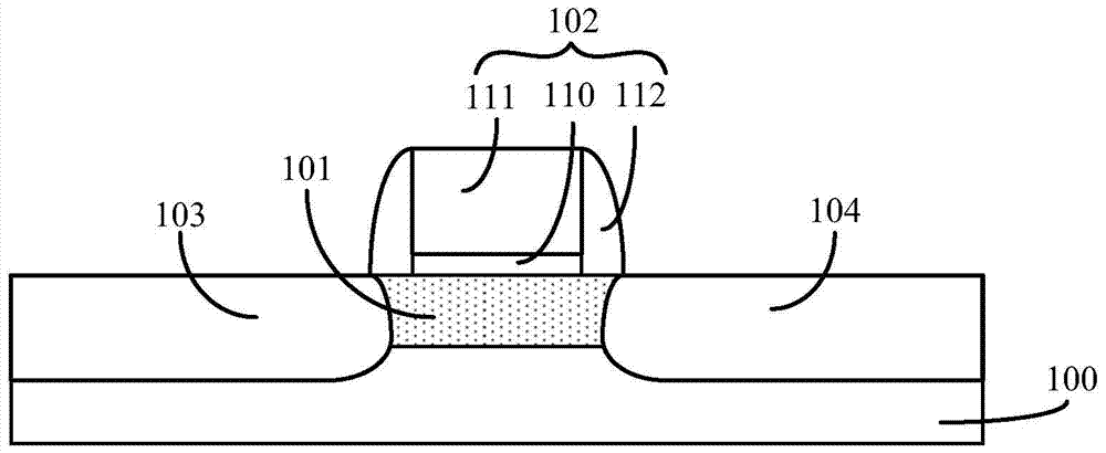
[0029] Such as figure 1 As shown, the existing junction-free transistors are planar transistors, so the size of the junction-free transistors is too large, which is not conducive to improving the integration of semiconductor devices.

[0030]In order to reduce the size of the junctionless transistor, after research, a transistor is proposed, including: a first doped region located on the surface of the semiconductor substrate, the first doped region has first doped ions, so The first doping ions in the first doping region have a first concentration; the semiconductor layer located on a part of the surface of the first doping region and has the first doping ions, the first doping ions in the semiconductor layer Has a first concentration; a second doped region located in the semiconductor layer, the second doped region is located on the sidewall and top surface of the semiconductor layer, and has a first doped region in the second doped region Ions, the first doping ions in the...


PUM


Abstract

A transistor and a forming method thereof are provided. The transistor comprises a semiconductor substrate, a semiconductor layer, a second doped region, a gate structure, and a drain region. The surface of the semiconductor substrate has a first doped region, the first doped region contains first doping ions, and the first doping ions in the first doped region have a first concentration. The semiconductor layer is disposed on part of the surface of the first doped region and contains first doping ions, and the first doping ions in the semiconductor layer have a first concentration. The second doped region is disposed in the semiconductor layer and on the surfaces of the side wall and the top of the semiconductor layer and contains first doping ions, and the first doping ions in the second doped region have a second concentration greater than the first concentration. The gate structure is disposed on the surface of the second doped region in the two side walls of the semiconductor layer. The drain region is disposed in part of the first doped region and part of the semiconductor substrate at the two sides of the semiconductor layer and the gate structure and contains first doping ions, and the first doping ions in the drain region have a second concentration. The transistor has a smaller size and higher degree of integration.

Description

technical field [0001] The invention relates to the technical field of semiconductor manufacturing, in particular to a transistor and a forming method thereof. Background technique [0002] With the rapid development of semiconductor manufacturing technology, semiconductor devices are developing towards higher element density and higher integration. As the most basic semiconductor device, transistors are currently being widely used. Therefore, with the increase of component density and integration of semiconductor devices, the gate size of planar transistors is getting shorter and shorter. The ability of traditional planar transistors to control channel current Weakened, it is easy to produce short channel effect and affect the electrical performance of semiconductor devices. [0003] In order to overcome the short-channel effect of transistors, a junction-less transistor (JLT, Junction-less Transistor) is proposed in the prior art. Please refer to figure 1 , figure 1 It...

Claims


Application Information

Patent Timeline
Patent Type & Authority Patents(China)
IPC IPC(8): H01L29/78H01L29/10H01L21/336
CPCH01L29/0847H01L29/1033H01L29/78
Inventor 刘金华
Owner SEMICON MFG INT (SHANGHAI) CORP
Why Eureka
Try Eureka