Processing method of printed circuit board

A technology of printed circuit boards and processing methods, which is applied in the directions of printed circuits, printed circuit manufacturing, and electrical connection formation of printed components, which can solve problems such as core board breakage and creases, and achieve the effect of high-density interconnection

Inactive Publication Date: 2015-03-18
SHENZHEN SUNTAK MULTILAYER PCB
View PDF6 Cites 19 Cited by
  • Summary
  • Abstract
  • Description
  • Claims
  • Application Information

AI Technical Summary

Problems solved by technology

[0005] The purpose of the present invention is to provide a method for processing printed circuit boards, which adopts the method of processing blind holes on the printed circuit board after lamination and filling the blind holes, aiming to solve the problems in the prior art before lamination. When drilling blind holes on the board, it is easy to break or crease the core board

Method used


Image

  • Processing method of printed circuit board
  • Processing method of printed circuit board
  • Processing method of printed circuit board

Examples


Embodiment Construction

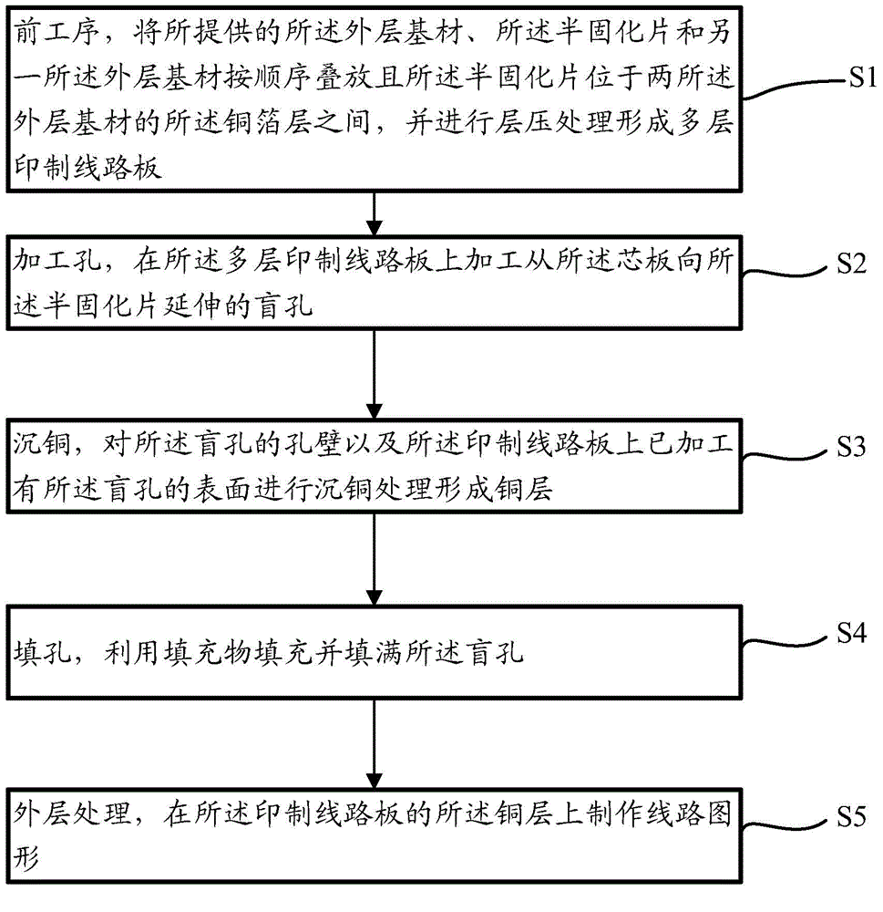
[0035] In order to make the object, technical solution and advantages of the present invention clearer, the present invention will be further described in detail below in conjunction with the accompanying drawings and embodiments. It should be understood that the specific embodiments described here are only used to explain the present invention, not to limit the present invention.

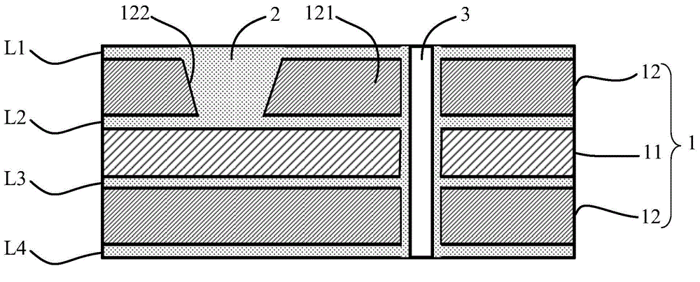
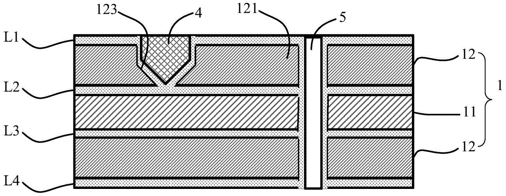
[0036] Please refer to Figure 1 to Figure 3 The method for processing printed circuit boards provided by the embodiment of the present invention at least provides an outer layer substrate 12, a prepreg 11 and another outer layer substrate 12, and the outer layer substrate 12 includes a core board 121 and is arranged on the The copper foil layer L1 and / or L2 on at least one surface of the core board 121 includes the following steps:

[0037] S1: the previous process, the provided outer substrate 12, the prepreg 11 and another outer substrate 12 are stacked in order, and the prepreg 11 is located b...


PUM


Abstract

The invention is applicable to the technical field of printed circuit boards and provides a processing method of a printed circuit board and aims at solving a problem, which exists in the prior art, that before lamination, when a blind hole is drilled in a core board, core board fracture or fold is likely to happen. The method includes the following steps: a pre-procedure: laminating an outer-layer substrate, a prepreg and another outer-layer substrate sequentially and carrying out lamination processing so as to form a multi-layer printed circuit board; hole processing: processing a blind hole, which extends from the core board to the prepreg, in the multilayer printed circuit board; copper deposition: carrying out copper deposition processing on the blind-hole printed circuit board so as to form a copper layer; hole filling: using a filler to fill the blind hole fully; and outer-layer processing: manufacturing a line pattern. Through blind-hole processing on the multilayer printed circuit board after the lamination processing and hole filling processing of the blind hole, electrical connection with the inner-layer core board is realized so that a problem that in a process of hole processing in the inner-layer core board, fracture or fold happens is solved so that realization of high-density interconnection of printed circuit boards is facilitated.

Description

technical field [0001] The invention belongs to the technical field of printed circuit boards, in particular to a processing method for printed circuit boards. Background technique [0002] With the rapid development of electronic technology, electronic products gradually tend to be miniaturized, lightweight, and highly integrated, and printed circuit boards are indispensable components of electronic products, which inevitably requires printed circuit boards to be small and lightweight and high density. The high density of printed circuit boards depends on the blind holes and lines connected between layers, and depends on the performance of electronic products. Therefore, the production of blind holes in printed circuit boards has become one of the keys to the development of printed circuit board technology. [0003] Generally, for a multi-layer printed wiring board, blind holes include blind holes extending from the outer surface of the printed wiring board to inner layers...

Claims


Application Information

Patent Timeline
Patent Type & Authority Applications(China)
IPC IPC(8): H05K3/42
CPCH05K3/421H05K2203/1438
Inventor 吴甲林彭卫红刘东黄海蛟
Owner SHENZHEN SUNTAK MULTILAYER PCB
Why Eureka
Try Eureka