
Packaging method and packaging structure of fan-out stacked chip

A technology of packaging structure and packaging method, which is applied in the manufacture of electrical components, electrical solid devices, semiconductor/solid devices, etc., can solve the problems of ultra-thin substrate production difficulty, difficulty, and unsustainable reduction, and achieve ultra-thin multi-layer Effects of high-density stacked packaging, reduced package size, and increased density interconnection

Pending Publication Date: 2022-03-11
NANTONG FUJITSU MICROELECTRONICS
View PDF0 Cites 1 Cited by
  • Summary
  • Abstract
  • Description
  • Claims
  • Application Information

AI Technical Summary

Problems solved by technology

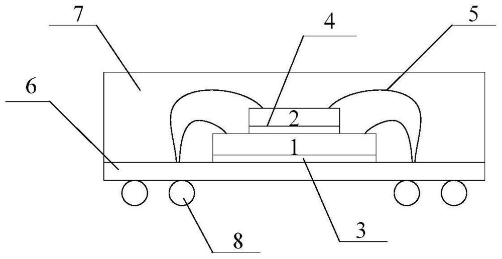
In the current packaging, due to the height limitation of the molding of the gold wire and the limitation of the protection distance from the molding compound to the gold wire, the height from the molding compound to the surface of the chip 2 is strictly limited and cannot be continuously reduced.
At the same time, the substrate process is extremely difficult to produce ultra-thin substrates due to material limitations and substrate strength limitations, which limit the application of traditional packaging in ultra-thin multi-layer packaging.
And whether it is traditional wire bonding connection or reverse soldering connection, the pad spacing is more than 30um, and it is extremely difficult to continue to shrink

Method used


Image

  • Packaging method and packaging structure of fan-out stacked chip
  • Packaging method and packaging structure of fan-out stacked chip
  • Packaging method and packaging structure of fan-out stacked chip

Examples


Embodiment Construction

[0041] In order to enable those skilled in the art to better understand the technical solutions of the present invention, the present invention will be further described in detail below in conjunction with the accompanying drawings and specific embodiments.

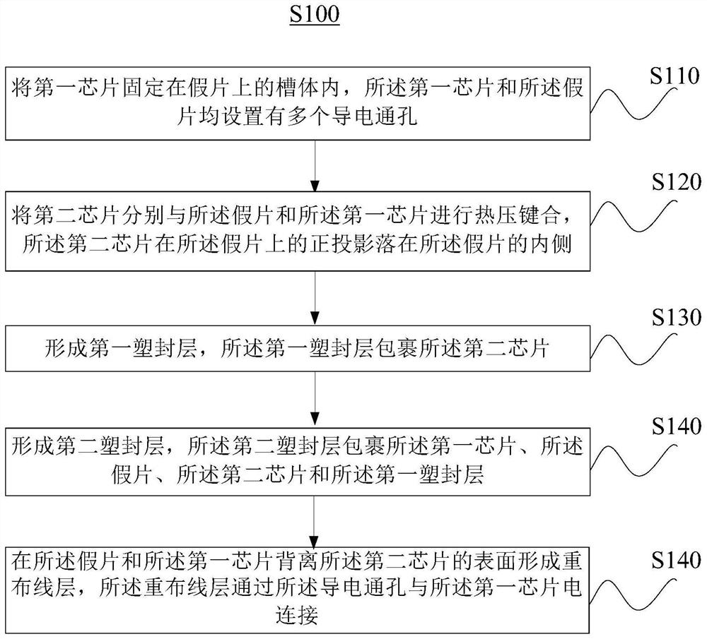
[0042] Such as figure 2 As shown, one aspect of the present invention provides a fan-out stacked chip packaging method S100, the packaging method S100 includes:

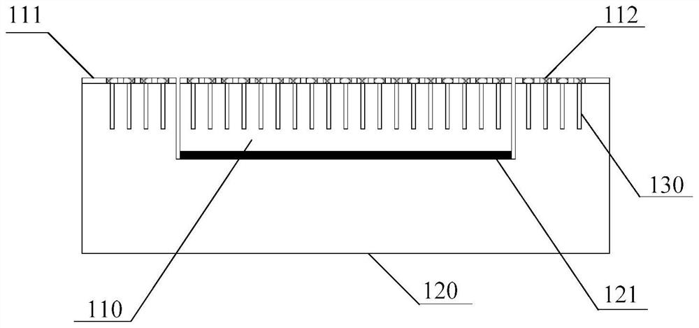
[0043] S110. Fix the first chip in the groove on the dummy, where the first chip and the dummy are both provided with a plurality of conductive through holes.

[0044] Specifically, such as image 3 As shown, the back side of the first chip 110 is fixed in the groove on the dummy 120 by the adhesive 121, wherein the surface of the first chip 110, that is, the front of the first chip 110 is flush with the surface of the dummy 120 In other words, the surface of the first chip 110 is flush with the surface of the dummy sheet 120 so as to better perform thermocom...


PUM


Abstract

The invention provides a fan-out stacked chip packaging method and packaging structure, and the method comprises the steps: enabling a first chip to be fixed in a groove body of a dummy chip, and enabling the first chip and the dummy chip to be provided with a plurality of conductive through holes; performing thermocompression bonding on the second chip with the dummy chip and the first chip, wherein the orthographic projection of the second chip on the dummy chip falls on the inner side of the dummy chip; forming a first plastic package layer, wherein the first plastic package layer wraps the second chip; forming a second plastic package layer, wherein the second plastic package layer wraps the first chip, the dummy chip, the second chip and the first plastic package layer; and forming a rewiring layer on the surfaces, deviating from the second chip, of the dummy chip and the first chip, wherein the rewiring layer is electrically connected with the first chip through the conductive through hole. According to the invention, the first chip and the second chip are respectively subjected to wafer expansion through the dummy wafer and the first plastic packaging layer, and then wafer-level thermocompression bonding is carried out, so that high-density interconnection is realized, and meanwhile, the production efficiency is improved. The packaging size is reduced through the conductive through holes and the fan-out rewiring technology, and ultra-thin multi-layer high-density stacked packaging is achieved.

Description

technical field [0001] The invention belongs to the technical field of semiconductor packaging, and in particular relates to a fan-out stacked chip packaging method and packaging structure. Background technique [0002] The size of electronic products is getting smaller and smaller, and their functions are getting stronger. Subsequently, semiconductor packages are required to be thinner and thinner, and the interconnection density is higher. Traditional packaging cannot meet future demands. figure 1 It is a typical traditional multi-layer chip packaging structure. Chips 1 and 2 are vertically stacked on a substrate 6 through patch films 3 and 4 , and chips 1 and 2 are connected to the substrate 6 through gold wires 5 . Chips 1, 2 and gold wire 5 are protected by plastic encapsulant 7. The entire package is connected to the outside world through solder balls 8 . In the current packaging, due to the limitation of the height of the molding of the gold wire and the limitatio...

Claims


Application Information

Patent Timeline
Patent Type & Authority Applications(China)
IPC IPC(8): H01L21/50H01L21/56H01L21/603H01L23/16H01L23/31H01L23/48H01L23/535
CPCH01L21/50H01L21/568H01L24/81H01L24/02H01L23/3135H01L23/16H01L23/481H01L23/535H01L2224/81H01L2224/02379
Inventor 杜茂华
Owner NANTONG FUJITSU MICROELECTRONICS
Learn More