
Printed circuit board and making method thereof

A technology of printed circuit board and manufacturing method, which is applied in the direction of multi-layer circuit manufacturing, printed circuit connected with non-printed electrical components, optical waveguide and light guide, etc., can solve the problems affecting the performance of optical fiber, and achieve the effect of preventing influence

Inactive Publication Date: 2009-06-10
JIANGNAN INST OF COMPUTING TECH
View PDF1 Cites 0 Cited by
  • Summary
  • Abstract
  • Description
  • Claims
  • Application Information

AI Technical Summary

Problems solved by technology

[0007] In the above technical solution, the optical fiber is directly embedded in the PCB. However, the PCB board needs to undergo lamination, tin-spraying and other board-making processes before application, as well as electronic assembly processes such as reflow soldering, which will easily affect the performance of the directly implanted optical fiber.

Method used


Image

  • Printed circuit board and making method thereof
  • Printed circuit board and making method thereof
  • Printed circuit board and making method thereof

Examples


Embodiment Construction

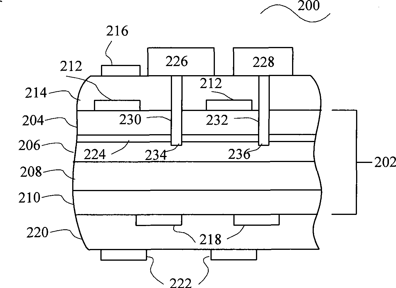
[0054] The invention embeds an optical channel structure in the stacked layer formed by stacking printed circuit board matrix boards, and implants optical fibers for optical interconnection after the printed circuit board manufacturing process is completed, preventing the printed circuit board manufacturing process from affecting the optical fiber performance.

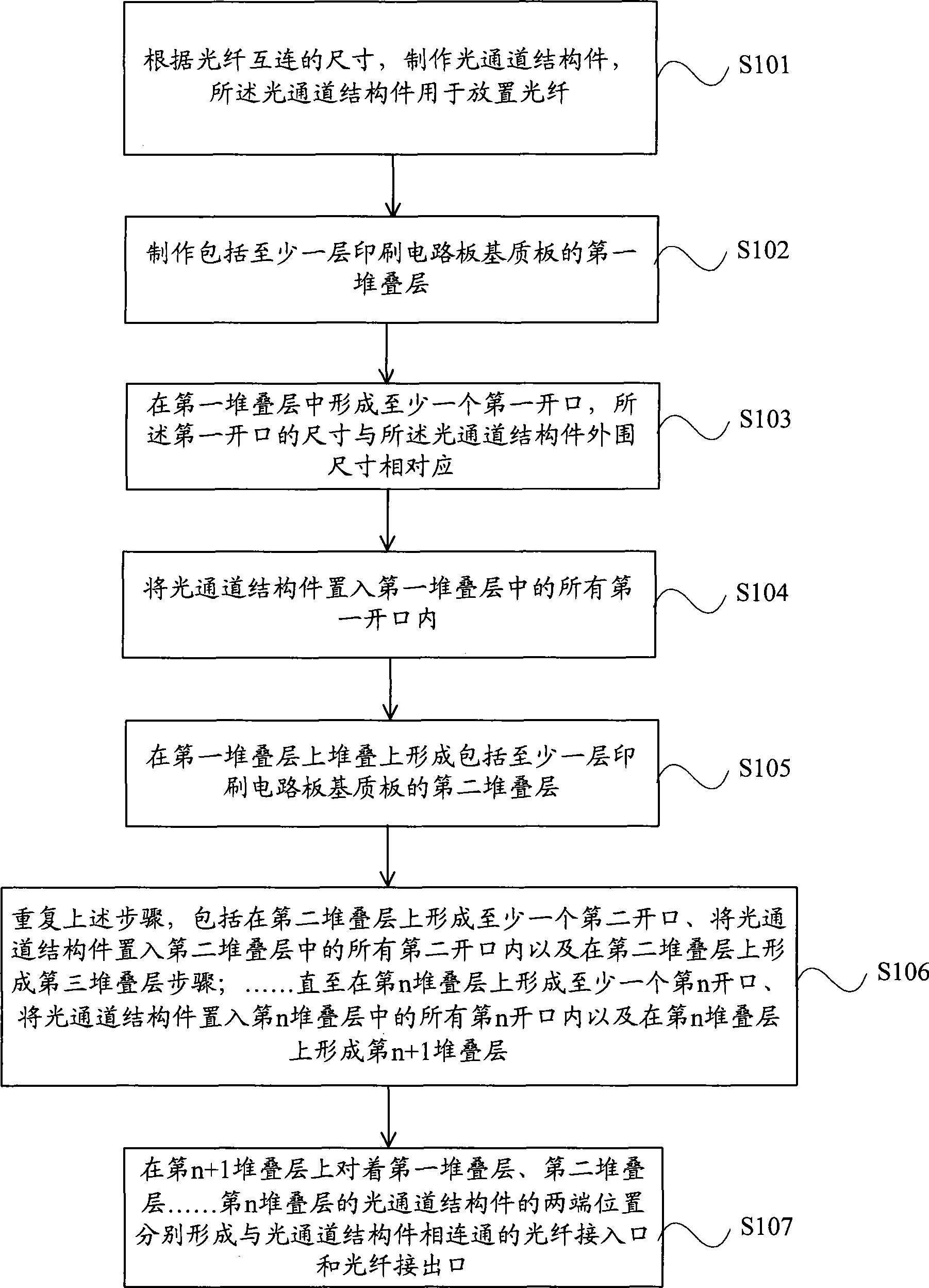
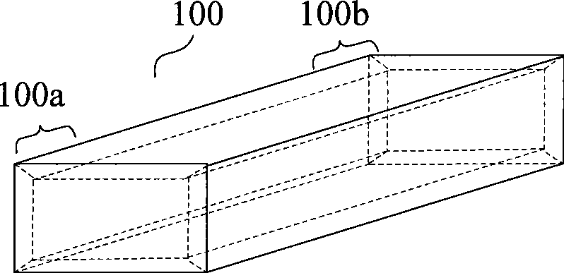
[0055] refer to figure 2 , the present invention provides a schematic flow chart of a specific embodiment of a printed circuit board, including the following steps: performing step S101, making a hollow and sealed optical channel structure of at least one size according to the size of the optical fiber interconnection, the optical The channel structure is used for built-in optical fibers; step S102 is performed to make a first stacked layer including at least one printed circuit board substrate board; step S103 is performed to form at least one first opening in the first stacked layer, the first opening The size corre...


PUM

PropertyMeasurementUnit
Bending radiusaaaaaaaaaa

Abstract

The invention discloses a method for manufacturing a printed circuit board. The method comprises the following steps: manufacturing at least one hollow and sealed optical channel structural member with one size according to sizes of optical fiber interconnection, wherein the optical channel structural member is used to embed an optical fiber; manufacturing a first stack layer which comprises at least one layer of a substrate sheet of the printed circuit board; forming at least one opening in the first stack layer; placing the optical channel structural members with different sizes into corresponding openings in the first stack layer; forming a second stack layer which comprises at least one layer of the substrate sheet of the printed circuit board on the stacks of the first stack layer; and forming an optical fiber inlet and an optical fiber outlet which are communicated with the optical channel structural members respectively at both ends facing to the optical channel structural member of the first stack layer on the second stack layer. The invention also provides the printed circuit board. The optical channel structural members are embedded in stack layers; and the optical fiber is embedded after manufacturing the printed circuit board to conduct optical connection. The printed circuit board prevents the process technology of the printed circuit board from influencing the optical fiber.

Description

technical field [0001] The invention relates to a printed circuit board, in particular to an optical fiber embedded printed circuit board and a manufacturing method thereof. Background technique [0002] A printed circuit board (PCB) is the basic component for connecting electronic components. The PCB is composed of a multilayer printed circuit board substrate board and a wire layer located between each layer of printed circuit board substrate boards. The multi-layer printed circuit board base plate is used as electrical insulation and mechanical support, and the wire layer is used for supplying power to electronic components on the PCB or interconnecting electrical signals between electronic components. [0003] With the development of a new generation of information equipment towards ultra-broadband, high-speed, large-capacity, and low-power consumption, the shortcomings of electrical signal interconnections are gradually emerging. For example, when transmitting high-spee...

Claims


Application Information

Patent Timeline
IPC IPC(8): H05K3/46H05K1/18G02B6/12
Inventor 陈文录张慧邬宁彪曾芳仔刘杰王鸿林
Owner JIANGNAN INST OF COMPUTING TECH
Learn More