Pixel structure and electrowetting display device comprising same

A pixel electrode and pixel technology, applied in the field of electrowetting display devices, can solve problems such as poor stability, achieve the effect of increasing storage capacitance and improving display stability

Active Publication Date: 2015-03-25
NANJING CEC PANDA LCD TECH
View PDF4 Cites 8 Cited by
  • Summary
  • Abstract
  • Description
  • Claims
  • Application Information

AI Technical Summary

Problems solved by technology

Therefore, compared with liquid crystal display, ele

Method used


Image

  • Pixel structure and electrowetting display device comprising same
  • Pixel structure and electrowetting display device comprising same
  • Pixel structure and electrowetting display device comprising same

Examples


Embodiment 1

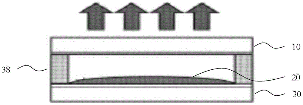
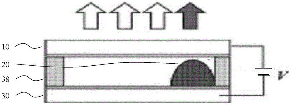
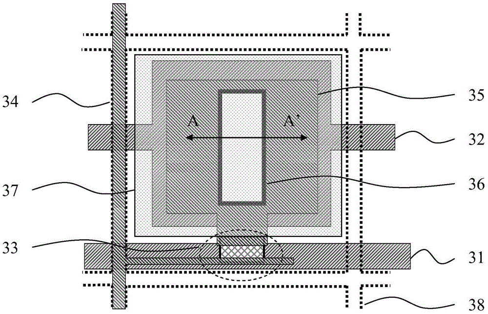
[0035] Figure 4 It is a schematic plan view of the pixel structure in Embodiment 1 of the present invention. Such as Figure 4 As shown, in the pixel structure, the storage capacitor is formed by the first metal layer M1, the gate insulating layer GI, the second metal layer M2, the passivation layer PAS, and the ITO transparent electrode layer. The size of the storage capacitor is increased through the double storage capacitor structure of the upper and lower layers, and the stability of the display is improved.

[0036] Such as Figure 4 As shown: the array substrate described in Embodiment 1 is sequentially distributed on the substrate as the scanning line 31 composed of the first metal layer M1, the common electrode connecting line segment 32a, and the metal pixel electrode 35; the array substrate composed of the second metal layer M2 Data line 34 , common electrode 32 b , pixel electrode connection line 39 . It also includes an extension of the data line 34 along the ...

Embodiment 2

[0047] Image 6 It is a schematic plan view of the pixel structure of Embodiment 2 of the present invention. Such as Image 6 As shown, in the pixel structure, the storage capacitor is formed by the metal layer M1, the gate insulating layer GI, the metal layer M2, the passivation layer PAS, and the ITO transparent electrode layer. The size of the storage capacitor is increased through the double storage capacitor structure of the upper and lower layers, and the stability of the display is improved.

[0048] Such as Image 6 As shown: the array substrate described in Embodiment 2 is sequentially distributed on the substrate as a scanning line 31 composed of the first metal layer M1, a common electrode connection line segment 32a, and a metal pixel electrode 35; Data line 34 , common electrode 32 b , pixel electrode connection line 39 . The scan line 31 , the semiconductor layer, the data line 34 , and the pixel electrode connection line 39 form a conventional thin film tran...


PUM


Abstract

The invention discloses a pixel structure and an electrowetting display device comprising the pixel structure. The pixel structure comprises a substrate. A first pixel electrode, a common electrode and a second pixel electrode are sequentially formed in a pixel region. A first storage capacitor is formed between the first pixel electrode and the common electrode. A second storage capacitor is formed between the common electrode and the second pixel electrode. By the adoption of the electrowetting display device comprising the pixel structure, maximization of the aperture ratio of pixels can be achieved, storage capacitance can also be enhanced, and the stability of electrowetting display is achieved.

Description

technical field [0001] The present invention relates to the field of display devices, in particular to a pixel and an electrowetting display device including the pixel. Background technique [0002] Electrowetting is one of the microfluidic phenomena, and the technology that uses the principle of electrowetting to realize display is the electrowetting display (Electro wetting Display, EWD) technology. Electrowetting display technology exploits the natural forces inherent in the oil-water interface and the display technologies developed to harness these forces. Specifically, the hydration of the hydrophobic surface of hydrophobic pigments such as dyed oil droplets is adjusted by applying a voltage, so that the dyed oil droplets spread evenly in the pixel when no voltage is applied, and are quickly pushed to the edge of the pixel after the voltage is applied, thereby realizing the color gray color. step display. [0003] The specific working principle of the EWD device is as...

Claims


Application Information

Patent Timeline
IPC IPC(8): G02B26/00
Inventor 时陶洪孟锋
Owner NANJING CEC PANDA LCD TECH
Why Eureka
Try Eureka