

Display panel, display device and manufacturing method of display panel
A display panel and manufacturing method technology, applied in the direction of instruments, semiconductor devices, optics, etc., can solve the problems of high probability of fragmentation and poor strength at OLB steps, and achieve the effects of reducing the probability of fragmentation, increasing strength, and improving stress concentration
- Summary
- Abstract
- Description
- Claims
- Application Information
AI Technical Summary
Problems solved by technology
Method used
Image

Examples
Embodiment Construction
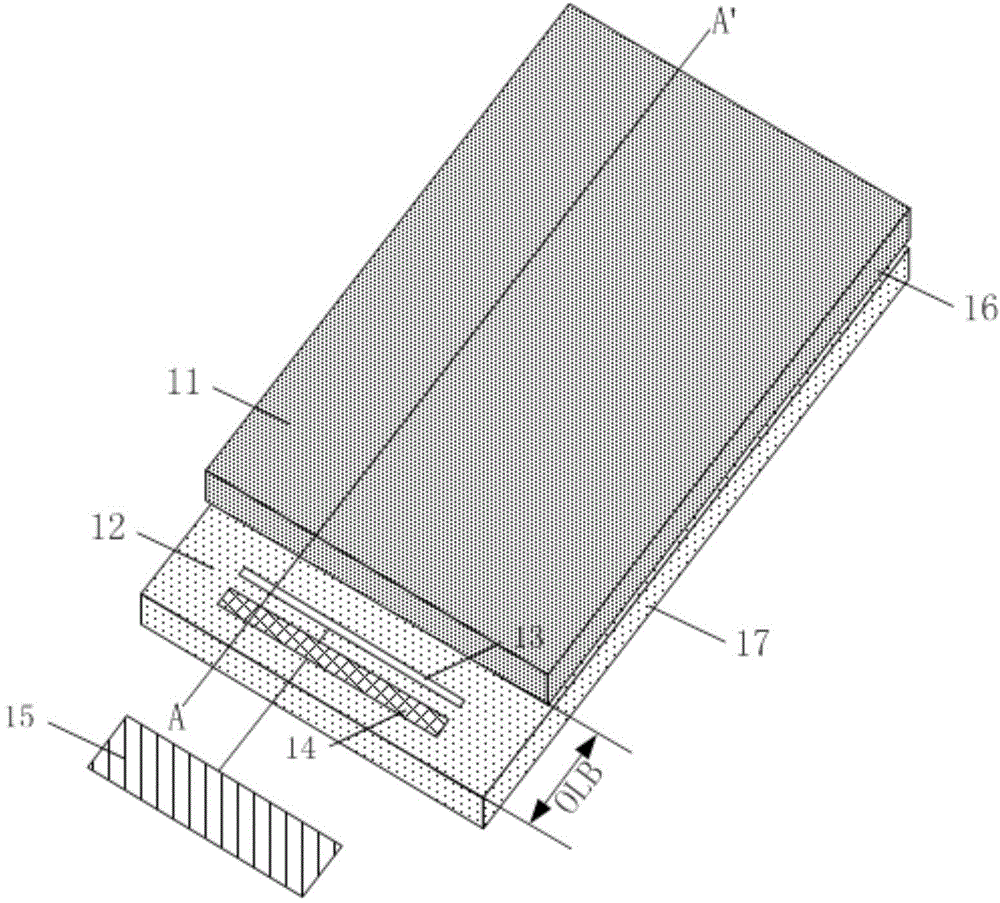
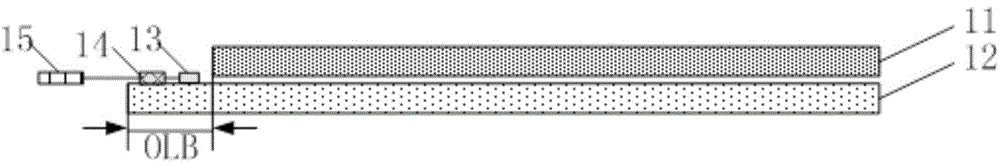
[0027] In order to make the purpose, technical solutions and advantages of the present invention clearer, the technical solutions of the present invention will be clearly and completely described through implementation with reference to the accompanying drawings in the embodiments of the present invention. Obviously, the described embodiments are the embodiment of the present invention. Some, but not all, embodiments. Based on the embodiments of the present invention, all other embodiments obtained by persons of ordinary skill in the art without making creative efforts belong to the protection scope of the present invention.
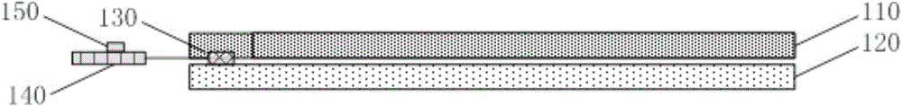
[0028] Referring to FIG. 2( a ), which is a schematic cross-sectional view of a display panel provided by an embodiment of the present invention, this embodiment can be applied to improve the stress concentration of the existing display panel and the situation that it is easy to break. In order to illustrate the structure of the display panel shown in FI...
PUM
 Abstract
Description
Claims
Application Information