Touch panel and manufacturing method thereof
A technology of a touch panel and a manufacturing method, which are applied in the directions of instruments, electrical digital data processing, and data processing input/output processes, etc., can solve the problems of inability of the sensing electrode layer and open circuit of the shielding layer.
- Summary
- Abstract
- Description
- Claims
- Application Information
AI Technical Summary
Problems solved by technology
Method used
Image
Examples
Embodiment Construction
[0015] The repeated symbols or signs may be used in the following different embodiments, and these repetitions are only for the purpose of simply and clearly describing the present invention, and do not represent any relationship between the different embodiments and / or structures discussed. Furthermore, when it is mentioned that a first material layer is located on or above a second material layer, it includes the situation that the first material layer is in direct contact with the second material layer or is separated by one or more other material layers. In the drawings, the shape or thickness of the embodiment may be exaggerated to simplify or highlight its features. In addition, components not shown or described in the figure can be in any form known to those skilled in the art.
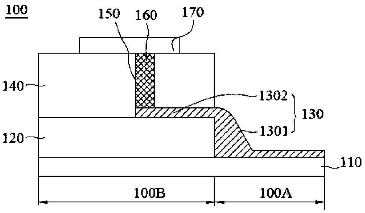
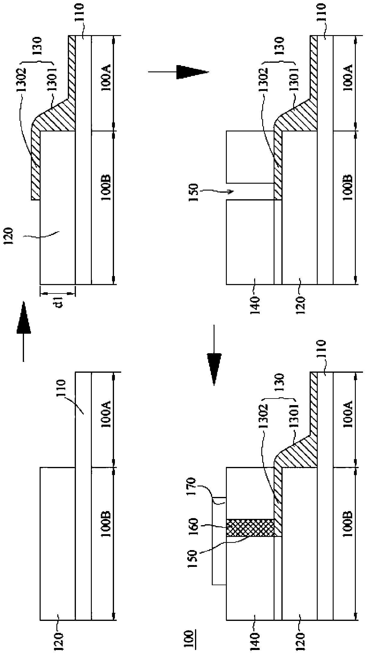
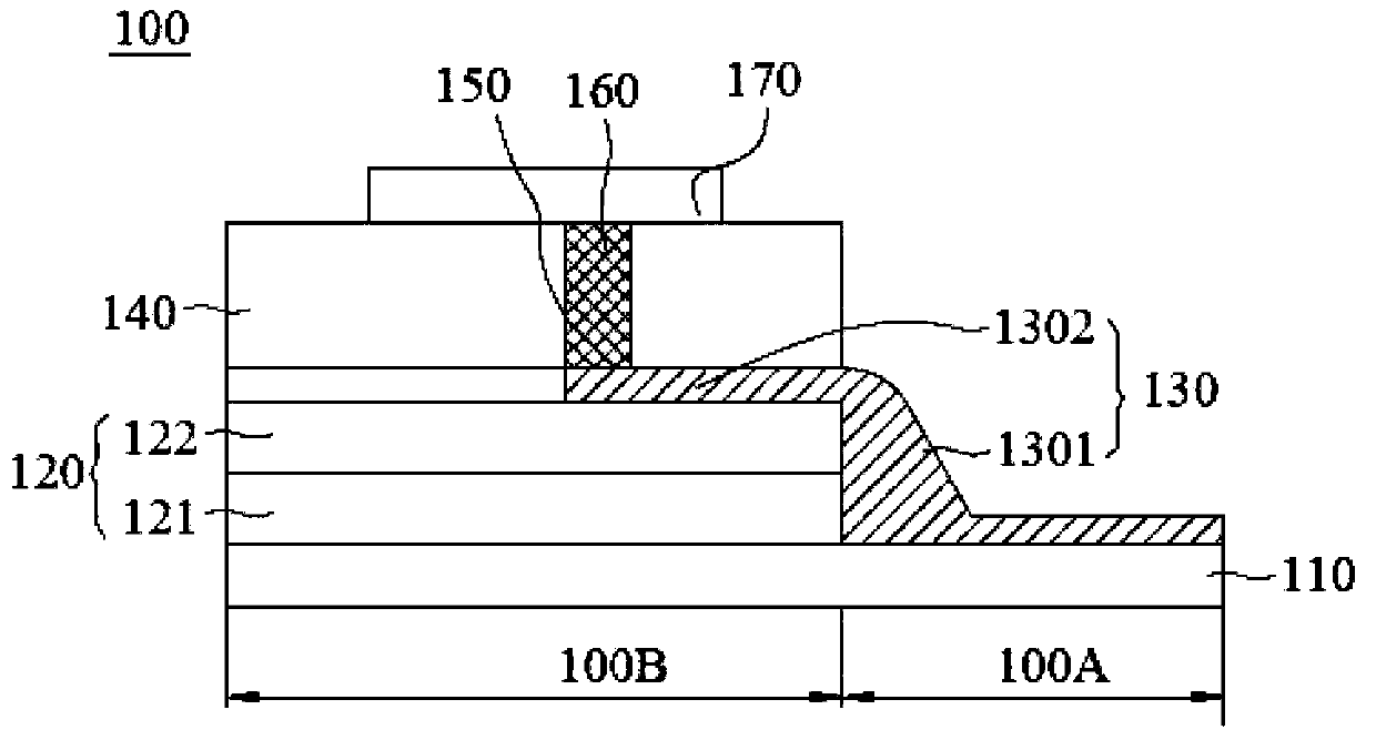
[0016] See figure 1 , shows a cross-sectional view of the touch panel according to the first embodiment of the present invention. like figure 1 As shown, the touch panel 100 is defined with ...
PUM
 Abstract
Description
Claims
Application Information


