Touch panel
A touch panel and touch area technology, applied in the direction of instruments, electrical digital data processing, electrical components, etc., can solve problems such as height drop, touch electrode disconnection, shortcut key or hot key touch function cannot be performed normally, etc. , to achieve the effect of reducing the delay of touch response
- Summary
- Abstract
- Description
- Claims
- Application Information
AI Technical Summary
Problems solved by technology
Method used
Image

Examples
Embodiment Construction
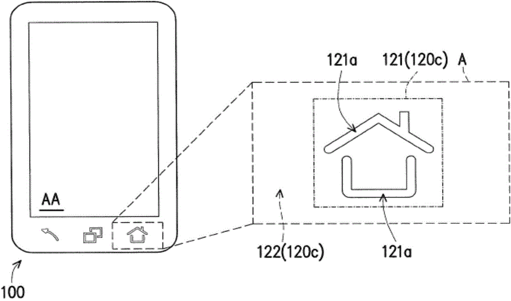
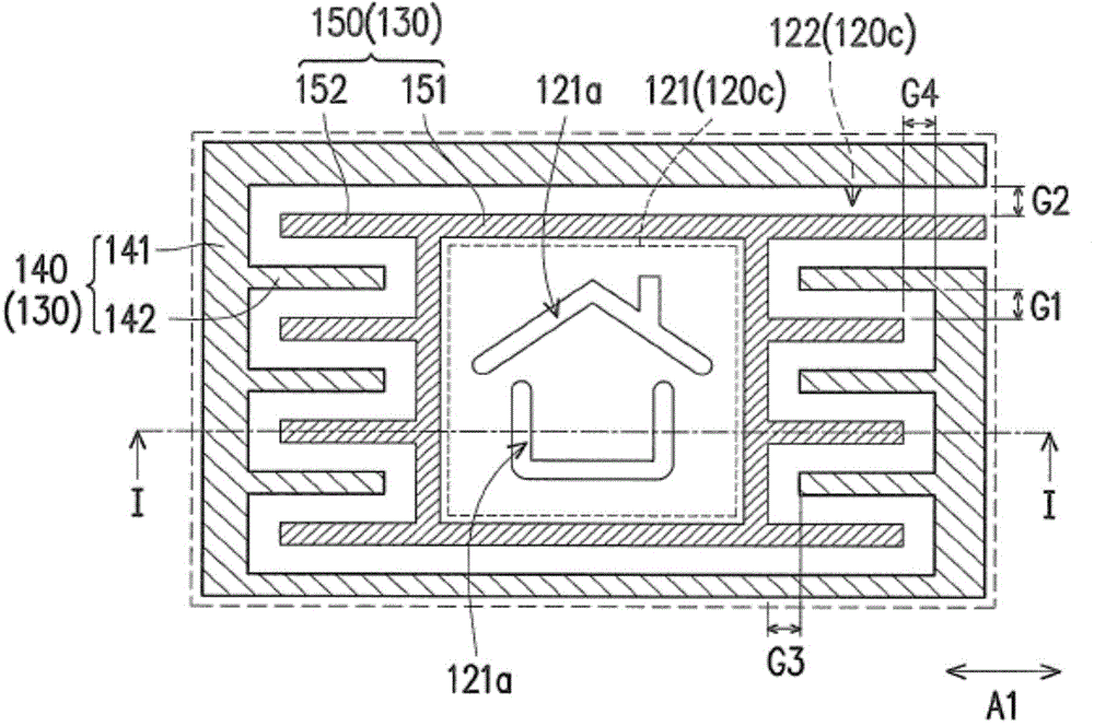
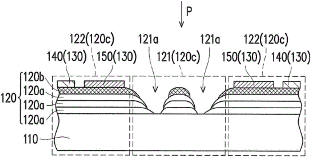
[0054] figure 1 is a schematic diagram of a touch panel according to an embodiment of the present invention. Figure 2A yes figure 1 Schematic diagram of the local layout of the conductive electrode structure in region A. Figure 2B yes Figure 2A a schematic sectional view along section line I-I, and for clarity of illustration, Figure 2B While the substrate 110 is drawn as the lowest layer, the size, relative size and shape of the various components, layers and regions may be exaggerated. Please refer to figure 1 , Figure 2A and Figure 2B , in this embodiment, the touch panel 100 includes a substrate 110 , at least one decoration layer 120 and a conductive electrode structure 130 . Specifically, the substrate 110 is, for example, a touch module of a smart phone or a tablet computer or a cover substrate of an electronic device, where the cover has the function of covering and protecting the touch module or the electronic device, and for example It is a transparent ...
PUM
 Abstract
Description
Claims
Application Information