Hole tamping method of circuit board

A circuit substrate and circuit board technology, which is applied in the direction of the electrical connection of printed components, can solve the problems of board surface depression, bubble rupture, and lower circuit board yield, so as to prevent board explosion, prevent depression, and improve yield. Effect

Inactive Publication Date: 2013-09-18
HONG HENG SHENG ELECTRICAL TECH HUAIAN +1
View PDF2 Cites 12 Cited by
  • Summary
  • Abstract
  • Description
  • Claims
  • Application Information

AI Technical Summary

Problems solved by technology

However, for circuit boards where the ratio of board thickness to conductive hole diameter is greater than or equal to 8, because the difference between the hole diameter and the board thickness is too far, it is often difficult to fill the plugging ink in the conductive hole by one screen printing to meet customer needs. , so it is often necessary to perform multiple plug holes through multiple screen printing to meet customer needs
Repeated screen printing will inevitably form air bubbles in the plugging ink. These bubbles are easy to expand at high temperature, which will lead to the phenomenon of board explosion. Then there is a depression, which reduces the yield of the circuit board

Method used


Image

  • Hole tamping method of circuit board
  • Hole tamping method of circuit board
  • Hole tamping method of circuit board

Examples


Embodiment Construction

[0020] The method for plugging holes of the circuit substrate provided by the technical solution will be further described in detail below with reference to the drawings and embodiments.

[0021] The plugging method of the circuit substrate provided by the technical solution comprises the steps of:

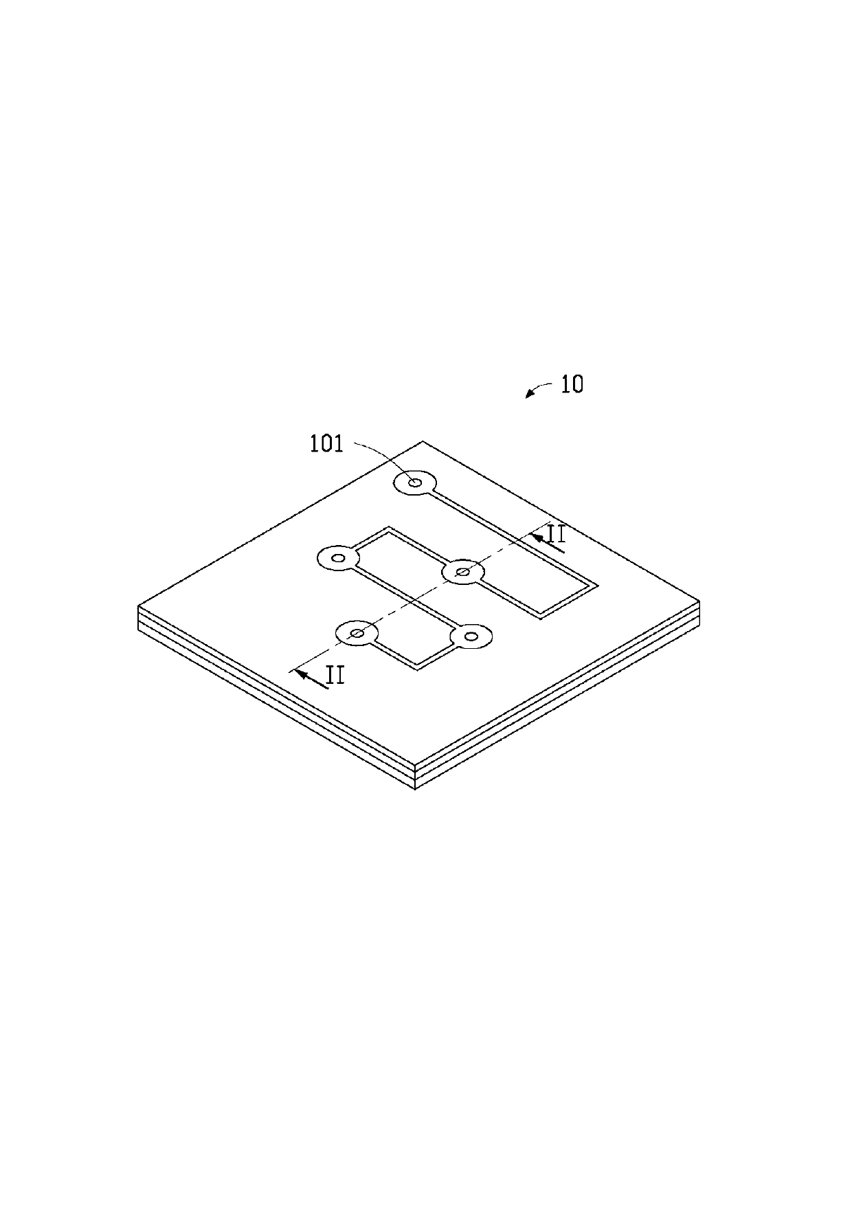
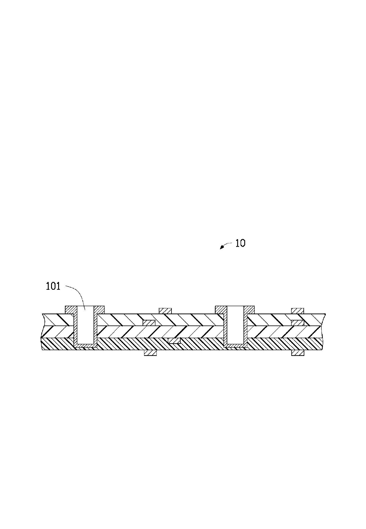
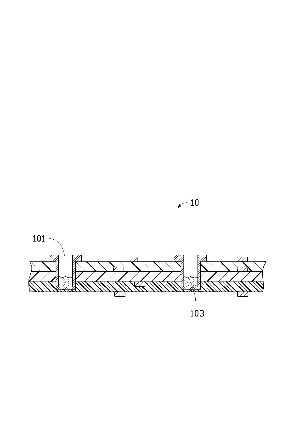
[0022] For a first step, see figure 1 and figure 2 , providing a circuit substrate 10 . The circuit substrate 10 is a structure including at least one insulating layer and at least one circuit layer. The circuit substrate 10 has a plurality of conductive holes 101 , the depth of each conductive hole 101 is greater than 3 mm, and the ratio of the thickness of the circuit substrate 10 to the depth of the conductive holes 101 is greater than or equal to 8. In this embodiment, the circuit substrate 10 is a four-layer circuit board, which includes three insulating layers and four circuit layers, the conductive hole 101 is a conductive blind hole, and the ratio of the thickness of t...


PUM


Abstract

The invention provides a hole tamping method of a circuit board. The method comprises the steps that the circuit board is provided, wherein the circuit board is provided with a number of conductive holes and the depth of each conductive hole is more than 3mm; through at least two hole tamping processes, a number of conductive holes are filled with hole tamping ink until each conductive hole is filled with the hole tamping ink, wherein each hole tamping process comprises the steps of filling the hole tamping ink in a number of conductive holes through screen printing and using ultrasonic to oscillate the circuit board with the conductive holes filled with the hole tamping ink for 30 seconds to 120 seconds to enable bubbles in the hole tamping ink to escape, wherein the filling depth of the hole tamping ink in each conductive hole is 1mm to 2mm; and ultrasonic is used to oscillate the circuit board with the conductive holes filled with the hole tamping ink for 30 seconds to 90 seconds, so as to acquire the circuit board with tamped holes. According to the hole tamping method provided by the technical scheme, more than two hole tamping processes and an additional oscillation process to eliminate the bubbles in the hole tamping ink, and the phenomenon of board detonation can be effectively prevented.

Description

technical field [0001] The invention relates to circuit board technology, in particular to a hole plugging method of a circuit substrate with better hole plugging effect. Background technique [0002] With the advancement of science and technology, circuit boards are widely used in electronic products. For the application of the circuit board, please refer to the literature Takahashi, A. Ooki, N. Nagai, A. Akahoshi, H. Mukoh, A. Wajima, M. Res. Lab, High density multilayer printed circuit board for HITAC M-880, IEEE Trans . on Components, Packaging, and Manufacturing Technology, 1992, 15(4): 418-425. [0003] Double-sided circuit boards and multi-layer circuit boards generally achieve electrical conduction between circuits of each layer through a conductive hole (Plated Through Hole, PTH). The production of conductive holes needs to go through processes such as punching and plugging, or through processes such as punching, blackening or electroless plating, electroplating, ...

Claims


Application Information

Patent Timeline
Patent Type & Authority Applications(China)
IPC IPC(8): H05K3/40
Inventor 白耀文
Owner HONG HENG SHENG ELECTRICAL TECH HUAIAN
Why Eureka
Try Eureka