Shallow trench isolation structure and forming method thereof

An isolation structure and shallow trench technology, which is applied in the manufacture of electrical components, electrical solid devices, semiconductor/solid devices, etc., can solve problems such as edge depressions and achieve the effect of improving yield

Active Publication Date: 2009-11-11
SEMICONDUCTOR MANUFACTURING INTERNATIONAL (BEIJING) CORP
View PDF1 Cites 11 Cited by
  • Summary
  • Abstract
  • Description
  • Claims
  • Application Information

AI Technical Summary

Problems solved by technology

[0014] The present invention provides a shallow trench isolation structure and its forming method to improve the phenomenon that the filler of the existing shallow trench isolation structure tends to have edge depressions after wet etching

Method used


Image

  • Shallow trench isolation structure and forming method thereof
  • Shallow trench isolation structure and forming method thereof
  • Shallow trench isolation structure and forming method thereof

Examples


no. 1 example

[0062] This embodiment introduces a method for forming a shallow trench isolation structure, Figure 5 A flowchart of a method for forming a shallow trench isolation structure according to the first embodiment of the present invention, Figure 6 to Figure 13 In order to illustrate the schematic cross-sectional view of the device of the method for forming the shallow trench isolation structure according to the first embodiment of the present invention, the following is combined with Figure 5 to Figure 13 The first embodiment of the present invention will be described in detail.

[0063] The method for forming a shallow trench isolation structure in this embodiment includes the steps of:

[0064] Step 501: Provide a substrate on which a stop layer has been formed.

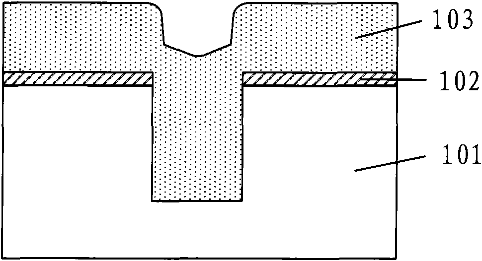
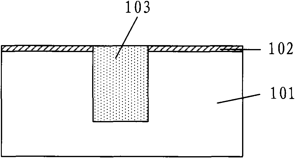
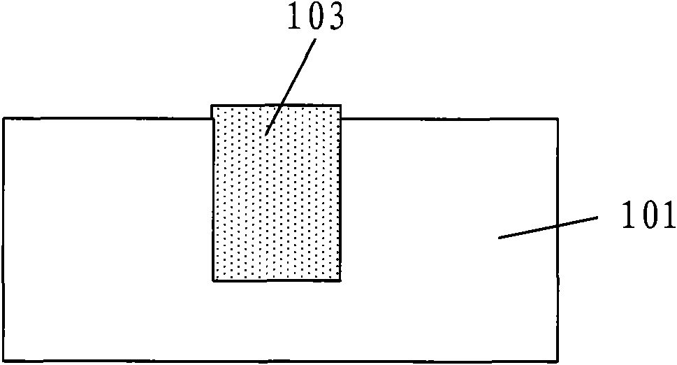
[0065] Image 6 It is a schematic cross-sectional view of the substrate in the first embodiment of the present invention, such as Image 6 As shown, the substrate provided in this embodiment is a silicon substra...

no. 2 example

[0096] This embodiment introduces a shallow trench isolation structure, Figure 14 It is a schematic cross-sectional view of the shallow trench isolation structure in the second embodiment of the present invention. like Figure 14As shown, the shallow trench isolation structure in this embodiment has a trench formed in the substrate 1401, the trench has a filler 1404, and there is also a gap between the inner sidewall of the trench and the filler 1404. There is a protective medium layer 1410 .

[0097] In this embodiment, the filler is silicon oxide formed by a high-density plasma chemical vapor deposition method, the protective medium layer can be a silicon nitride layer or a silicon oxynitride layer, and the growth thickness of the protective medium layer can be exist to between, if Wait.

[0098] Considering that in the process of device formation, introducing a material layer with stress can improve device characteristics. For example, compressive strain along th...


PUM


Abstract

The invention discloses a forming method of a shallow trench isolation structure, comprising the steps: providing an substrate; forming a stop layer on the substrate; defining a shallow trench graph on the substrate; forming a trench in the substrate on which the stop layer is formed; depositing protective dielectric layers on the stop layer and the trench; corroding the protective dielectric layers until the protective dielectric layer on the stop layer is removed; depositing filler on the stop layer and in the trench; performing planarization process on the substrate where the filler is deposited; eliminating the stop layer on the substrate; and processing the filler by a method of wet etching. The invention also discloses the corresponding shallow trench isolation structure. The shallow trench isolation structure and the forming method thereof can prevent pits occurring at the edges of the shallow trench isolation structure, thereby the forming quality of the shallow trench isolation structure and the yield of devices are improved.

Description

technical field [0001] The present invention relates to the technical field of semiconductor manufacturing, in particular to a shallow trench isolation structure and a method for forming the same. Background technique [0002] With the continuous reduction of the feature size of semiconductor devices, the isolation area between devices is correspondingly reduced, and the requirements for device isolation are getting higher and higher. The local field oxidation isolation technology (LOCOS, Local Oxidation of Silicon) used in the early stage It will form a "bird's beak" (BIRD'S BEAK) region at the boundary of the active region, and the problems such as the expansion of the separation region have been gradually replaced by Shallow Trench Isolation (STI). Using the STI technology to prepare an isolation region to achieve isolation between devices has the advantage that the line width of the active region can be used most effectively and the integration degree can be improved. ...

Claims


Application Information

Patent Timeline
Patent Type & Authority Applications(China)
IPC IPC(8): H01L21/762H01L27/02
Inventor 张海洋陈海华黄怡何其旸
Owner SEMICONDUCTOR MANUFACTURING INTERNATIONAL (BEIJING) CORP
Why Eureka
Try Eureka