Semiconductor structure and formation method thereof

A semiconductor and fin technology, applied in the field of semiconductor structure and its formation, can solve the problems that the performance of semiconductor structure needs to be improved

Active Publication Date: 2019-06-07
SEMICON MFG INT (SHANGHAI) CORP +1
View PDF4 Cites 3 Cited by
  • Summary
  • Abstract
  • Description
  • Claims
  • Application Information

AI Technical Summary

Problems solved by technology

[0004] However, the performance of semiconductor structures in the prior art still needs to be improved

Method used


Image

  • Semiconductor structure and formation method thereof
  • Semiconductor structure and formation method thereof
  • Semiconductor structure and formation method thereof

Examples


Embodiment Construction

[0033] It can be seen from the background art that the performance of existing semiconductor structures still needs to be improved.

[0034] Now combined with a method of forming a semiconductor structure for analysis, Figure 1 to Figure 5 It is a structural diagram corresponding to each step in a method for forming a semiconductor structure. The process steps for forming a semiconductor structure mainly include:

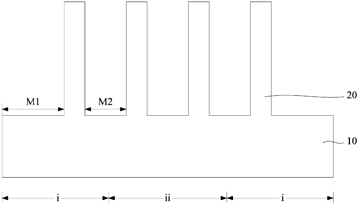
[0035] refer to figure 1 , providing a substrate 10 and fins 20 protruding from the substrate 10 .

[0036] The substrate 10 includes an edge region i and a central region ii between adjacent edge regions i.

[0037] There are multiple fins 20 , and the multiple fins 20 are arranged at equal intervals on the substrate 10 . The distance between the fin 20 in the edge region i and the sidewall of the substrate 10 is a first distance M1, and the distance between the fin 20 in the edge region i and an adjacent fin 20 is a second distance M2 , M1≠M2.
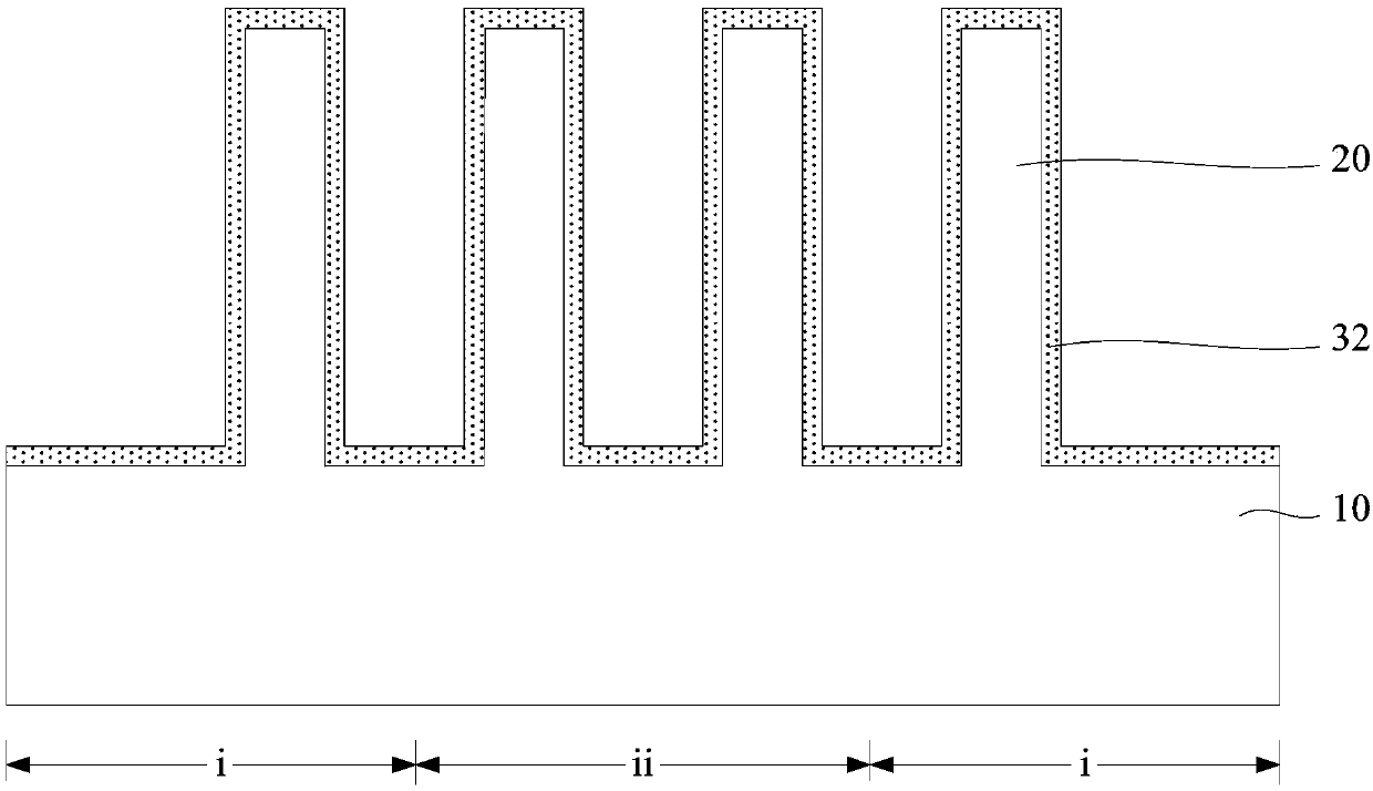
[0038] refer...


PUM


Abstract

The present invention provides a semiconductor structure and a formation method thereof. The method comprises the steps of: providing a substrate and fins protruding from the substrate, wherein each fin comprises a fin first portion located at the surface of the substrate and a fin second portion located at the top portion of the fin first portion; forming first laying layers at the side walls ofthe fin first portions; forming second laying layers at the surfaces of the first laying layers and the top portions and the side walls of the fin second portions; forming isolation films covering thesecond laying layer on the substrate, wherein the top portions of the isolation films are higher than the top portions of the fins and are levelled with the top portions of the fins; removing the second laying layers and the isolation films higher than the top portions of the fin first portions, wherein the remaining isolation films form isolation layers; and forming gate oxide layers at the surfaces of the top portions and the side walls of the fins exposed on the isolation layers. In the invention, the first laying layers and the second laying layers can effectively weaken the stress applied to the side walls of the fins so as to avoid bending of the fins, and the formed process window of the isolation layers is large which facilitates improvement of the formation quality of the isolation layers.

Description

technical field [0001] The invention relates to the technical field of semiconductor manufacturing, in particular to a semiconductor structure and a forming method thereof. Background technique [0002] In semiconductor manufacturing, as the feature size of integrated circuits continues to decrease, the channel length of MOSFETs has also been shortened accordingly. However, as the channel length of the device is shortened, the distance between the source and the drain of the device is also shortened, resulting in poor control ability of the gate to the channel, and short-channel effects (SCE: short-channel effects) more likely to happen. [0003] The Fin Field Effect Transistor (FinFET) has outstanding performance in suppressing the short channel effect. The gate of the FinFET can control the fin at least from both sides. Therefore, compared with the planar MOSFET, the gate of the FinFET has an The control ability is stronger, and the short channel effect can be well suppr...

Claims


Application Information

Patent Timeline
Patent Type & Authority Applications(China)
IPC IPC(8): H01L29/78H01L21/336H01L29/423
Inventor 周飞
Owner SEMICON MFG INT (SHANGHAI) CORP
Why Eureka
Try Eureka