Semiconductor device and method for producing same

A manufacturing method and semiconductor technology, applied in semiconductor/solid-state device manufacturing, semiconductor devices, transistors, etc., can solve the problem of not easily improving the pixel aperture ratio, and achieve the effect of high yield

Active Publication Date: 2015-04-08
SHARP KK
View PDF7 Cites 5 Cited by
  • Summary
  • Abstract
  • Description
  • Claims
  • Application Information

AI Technical Summary

Problems solved by technology

[0006] Especially in small, high-resolution liquid crystal display devices used in smartphones, etc., it is difficult to increase the aperture ratio of pixels due to restrictions on the minimum width of wiring (process rules), etc.

Method used


Image

  • Semiconductor device and method for producing same
  • Semiconductor device and method for producing same
  • Semiconductor device and method for producing same

Examples


Embodiment approach 1

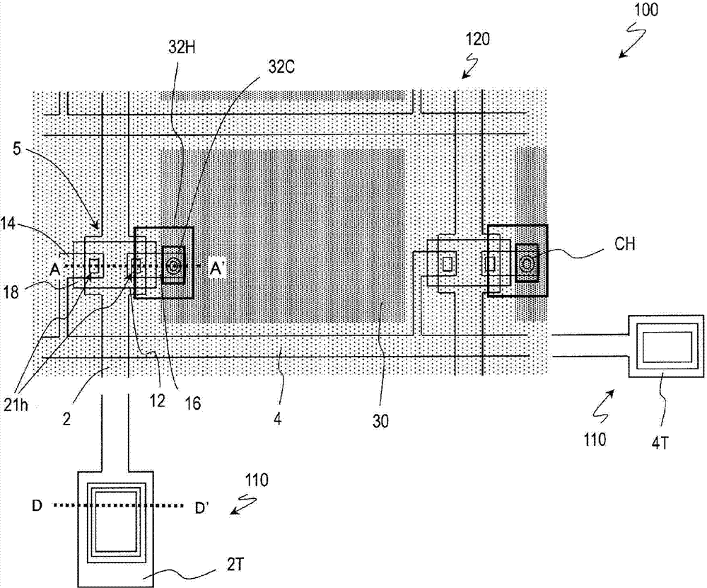
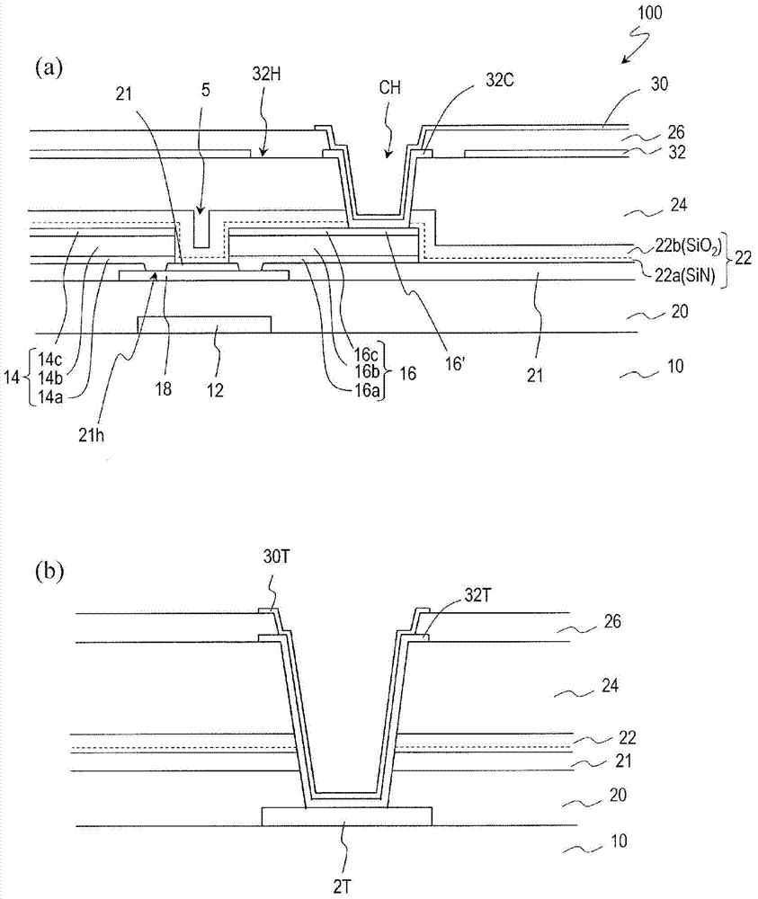
[0055] figure 2 and image 3 (a) and (b) represent the semiconductor device 100 of the first embodiment. Here, the semiconductor device 100 is a TFT substrate (active matrix substrate) 100 used in a liquid crystal display device. figure 2 An example of the planar structure of the TFT substrate 100 is schematically shown, image 3 (a) and (b) represent respectively along figure 2 The section of the line A-A' and along the figure 2 The cross-section of the D-D' line.

[0056] Such as figure 2 As shown, the TFT substrate 100 has: a display region (active region) 120 contributing to display; and a peripheral region (frame region) 110 located outside the display region 120 .

[0057] A plurality of gate wirings 2 and a plurality of source wirings 4 are provided in the display region 120 , and each region surrounded by these wirings becomes a "pixel". A plurality of pixels are arranged in a matrix, and in each pixel, a thin film transistor (TFT) 5 as an active element is...

Embodiment approach 2

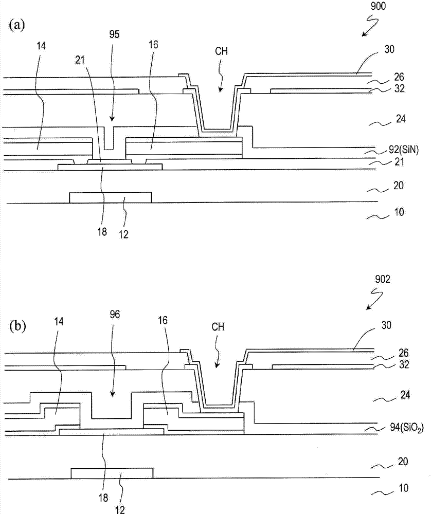
[0108] Figure 7 and Figure 8 (a) and (b) show the TFT substrate 200 of the second embodiment. The TFT substrate 200 of this embodiment differs from the TFT substrate 100 of Embodiment 1 in that the etching stopper layer 24 is not formed on the oxide semiconductor layer 18 . That is, the TFT substrate 200 of the present embodiment includes a channel-etched TFT 6 . In addition, the same reference numerals are assigned to the same components as those in Embodiment 1, and description thereof will be omitted.

[0109] Such as Figure 8 As shown in (a) and (b), in the TFT substrate 200, the passivation layer 23 provided to cover the TFT 6 is provided in contact with the source electrode 14 and the drain electrode 16, and is provided in contact with the oxide semiconductor layer 18. The channel region is also in contact.

[0110] In the present embodiment, the passivation layer 23 includes the lower insulating layer 23 a and the upper insulating layer 23 b provided on the lowe...


PUM

PropertyMeasurementUnit
thicknessaaaaaaaaaa
thicknessaaaaaaaaaa
thicknessaaaaaaaaaa

Abstract

A semiconductor device (100) is provided with a gate electrode (12) formed on a substrate (10), a gate insulating layer (20) formed on the gate electrode, an oxide semiconductor layer (18) formed on the gate insulating layer, a source electrode (14) and a drain electrode (16) connected to the oxide semiconductor layer, and an insulating layer (22) formed on the source electrode and the drain electrode. The insulating layer has: a silicon nitride layer (22a) that is connected to at least portions of the tops of the source electrode and the drain electrode, and has thickness of over 0 nm but not more than 30 nm; and a silicon oxide layer (22b) formed on the silicon nitride layer and having a thickness of over 30 nm.

Description

technical field [0001] The present invention relates to a semiconductor device (such as an active matrix substrate) fabricated using an oxide semiconductor and a method of manufacturing the same. Background technique [0002] Active matrix substrates used in liquid crystal display devices and the like include switching elements such as thin film transistors (Thin Film Transistor: hereinafter referred to as “TFT”) for each pixel. As such a switching element, a TFT having an amorphous silicon film as an active layer (active layer) (hereinafter referred to as "amorphous silicon TFT") and a TFT having a polysilicon film as an active layer (hereinafter referred to as TFT) have been widely used. as "polysilicon TFT"). [0003] In recent years, attempts have been made to use materials other than amorphous silicon and polysilicon as the material of the active layer of the TFT. For example, Patent Document 1 describes a liquid crystal display device in which an active layer of a TF...

Claims


Application Information

Patent Timeline
Patent Type & Authority Applications(China)
IPC IPC(8): H01L21/336G02F1/1368H01L21/28H01L29/417H01L29/786
CPCH01L29/7869H01L29/458H01L27/1225G02F1/1368H01L29/41733H01L29/78606H01L21/02164H01L21/0217H01L21/02274H01L21/441H01L29/24H01L29/45H01L29/66969H01L21/02565H01L21/477H01L29/78618
Inventor 美崎克纪
Owner SHARP KK
Why Eureka
Try Eureka