Analog switch circuit

A switching circuit and circuit technology, applied in electronic switches, electrical components, pulse technology, etc., can solve problems such as inability to optimize switching characteristics

Active Publication Date: 2019-09-03
REALTEK SEMICON CORP
View PDF19 Cites 0 Cited by
  • Summary
  • Abstract
  • Description
  • Claims
  • Application Information

AI Technical Summary

Problems solved by technology

[0004] In view of the problems of the above-mentioned prior art, the object of the present invention is to provide an analog switch circuit to solve the problem that the switching characteristics cannot be optimized

Method used


Image

  • Analog switch circuit
  • Analog switch circuit
  • Analog switch circuit

Examples


Embodiment Construction

[0043] In order for the examiner to understand the technical features, content and advantages of the present invention and the effects it can achieve, the present invention is hereby combined with the accompanying drawings and described in detail in the form of embodiments as follows, and the drawings used therein are, Its purpose is only for illustration and auxiliary instructions, not necessarily the true proportion and precise configuration of the present invention after implementation, so the proportion and configuration relationship of the attached drawings should not limit the patent scope of the present invention in actual implementation. Explain first.

[0044] Embodiments of the analog switch circuit according to the present invention will be described below with reference to related drawings. For ease of understanding, the same components in the following embodiments are described with the same symbols.

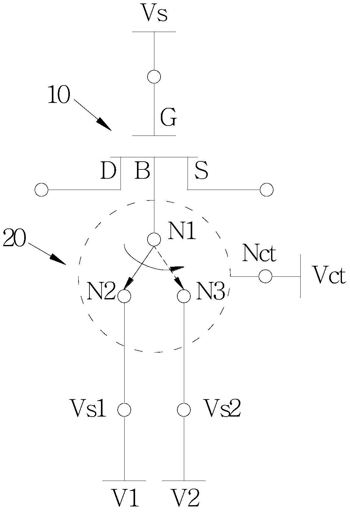
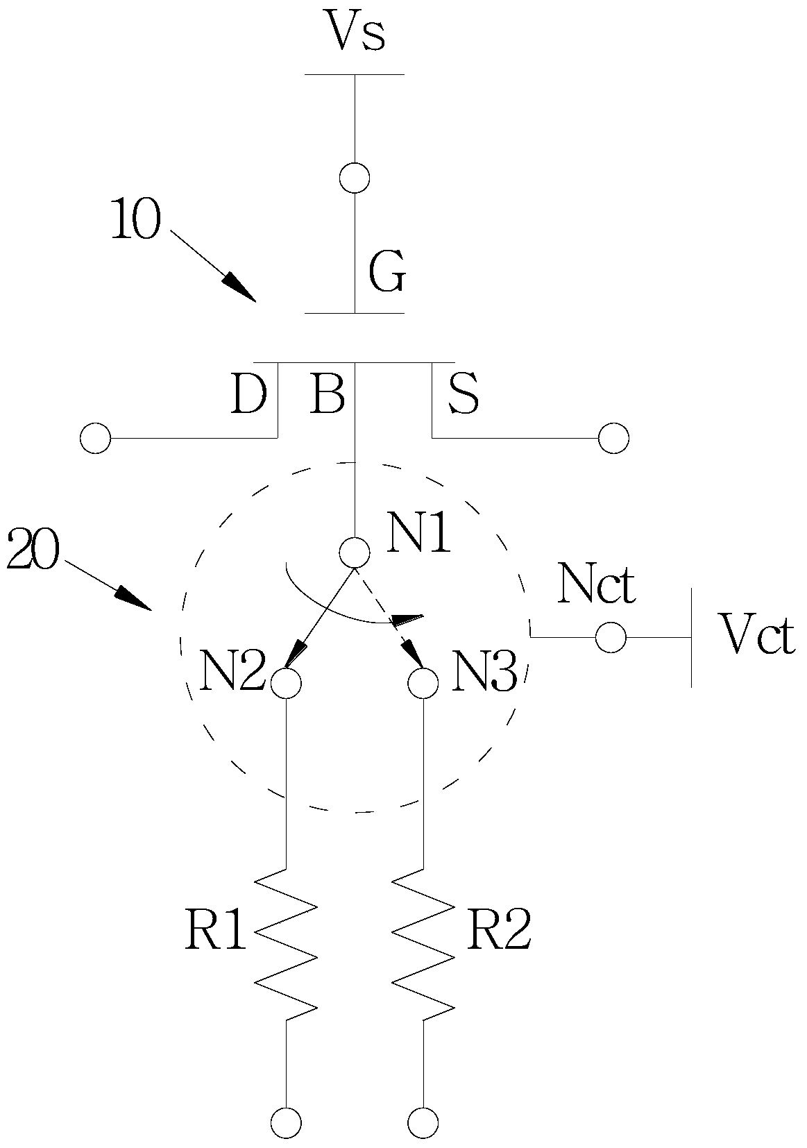
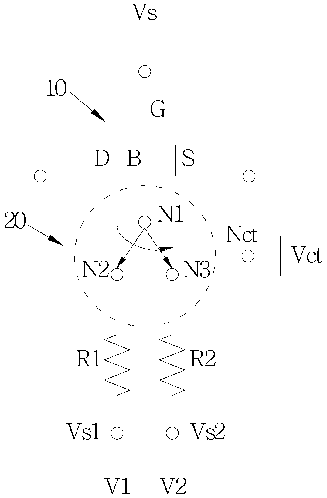
[0045] see figure 1 , which is a schematic diagram of the fir...


PUM


Abstract

Disclosed in the invention is an analog switch circuit for a high-frequency signal. The analog switch circuit comprises a metal-oxide-semiconductor field-effect transistor and a control switch. The metal-oxide-semiconductor field-effect transistor consists of a drain electrode, a source electrode, a gate electrode and a polar electrode. A gate bias voltage is applied to the gate electrode to control conduction or disconnection of the metal-oxide-semiconductor field-effect transistor. The control switch consists of a control terminal, a first terminal, a second terminal and a three terminal; and the first terminal is connected to the polar electrode. A control bias voltage related to the gate bias voltage is applied to the control terminal, so that the first terminal is connected to the second terminal when the metal-oxide-semiconductor field-effect transistor is in a conduction state and the first terminal is connected to the third terminal when the metal-oxide-semiconductor field-effect transistor is turned off. The second terminal is connected to a first voltage source providing a first bias voltage; and the third terminal is connected to a second voltage source providing a second bias voltage different from the first bias voltage.

Description

technical field [0001] The present invention discloses an analog switch circuit, especially an analog switch circuit which can optimize circuit characteristics according to the switch state. Background technique [0002] Because it is easy to miniaturize, can be integrated in the manufacturing process, and has good component characteristics, when an analog switch is to be set in a communication system, a metal-oxidation-semiconductor field-effect transistor (MOSFET) is often used ) to achieve, and the switch on or off can be controlled by the bias applied to the gate. When the switch is turned on, a carrier channel (N-type or P-type) is formed between the drain and the source of the metal oxide semiconductor field effect transistor. At this time, the drain and the source can be equivalent to a resistance. When the switch is turned off, there is no or only a very narrow carrier channel between the drain and the source of the metal oxide semiconductor field effect transistor....

Claims


Application Information

Patent Timeline
Patent Type & Authority Patents(China)
IPC IPC(8): H03K17/687
Inventor 陈冠宇陈力辅
Owner REALTEK SEMICON CORP
Why Eureka
Try Eureka