

Solid-state imaging device, method of manufacturing solid-state imaging device, and electronic device
A solid-state imaging device and pixel technology, which is applied in radiation control devices, circuits, electrical components, etc., can solve the problems of optical color mixing and degradation of focus characteristics, and achieve improved image quality, improvement of focus characteristics, and reduction of optical color mixing Effect
Active Publication Date: 2018-11-09
SONY CORP
View PDF5 Cites 0 Cited by
- Summary
- Abstract
- Description
- Claims
- Application Information
AI Technical Summary
Problems solved by technology
[0005] In this case, it is preferable to form a light-shielding film between the light-receiving parts on the back surface side of the substrate forming the light-input side, but since the distance between the substrate and the surface of the condenser lens increases in proportion to the height of the light-shielding film, Possibility of deteriorating focus characteristics
In addition, due to the oblique input light from the insulating film located between the substrate provided with the photoelectric conversion part and the light shielding film, there will be a problem of optical color mixing.
Method used
View moreImage
Smart ImageViewing Examples

Examples
no. 1 example
[0047] 1. First embodiment: Solid-state imaging device
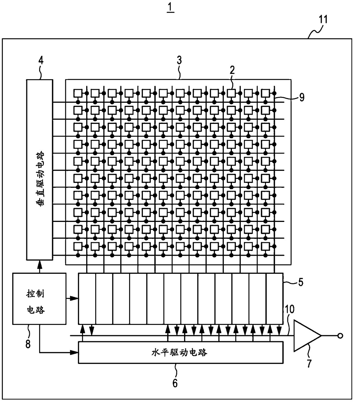
[0048] 1-1 Overall structure of solid-state imaging device
[0049] 1-2 Structure of main parts
[0050] 1-3 Method of manufacturing solid-state imaging device
[0051] 1-4 Comparison example
[0052] 1-5 Modification example
[0053] 1-6 Method of Manufacturing Solid-State Imaging Device According to Modified Example
no. 2 example
[0054] 2. Second Embodiment: Solid-state Imaging Device
[0055] 2-1 Structure of main parts
[0056] 2-2 Method of manufacturing solid-state imaging device
no. 3 example
[0057] 3. Third Embodiment: Solid-state Imaging Device
[0058] 3-1 Structure of main parts
[0059] 3-2 Method of manufacturing solid-state imaging device
[0060] 3-3 Modification example
Login to View More PUM
 Abstract
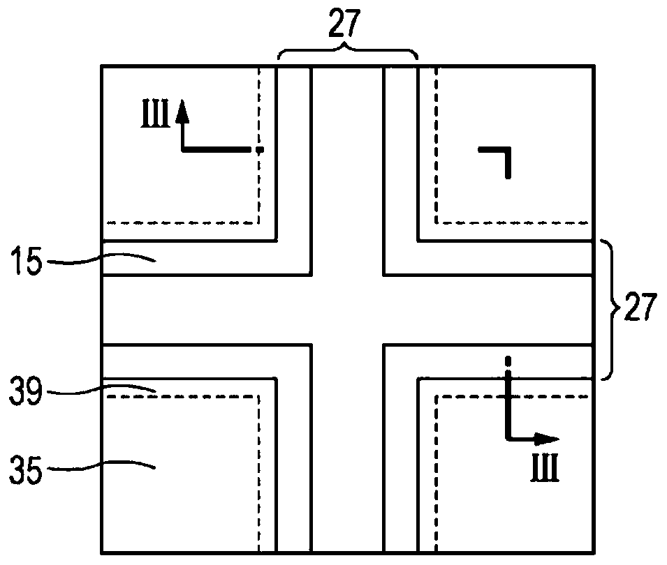
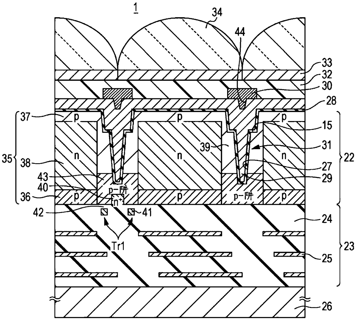
Provided are a solid-state imaging device (1), a method of manufacturing the solid-state imaging device, and electronic equipment. A solid-state imaging device includes a substrate (22) in which a plurality of pixels (2) are formed. In addition, a plurality of grooves (27) are formed in the substrate, particularly in pixel isolation regions (31) between adjacent pixels. The groove extends from the first surface of the substrate toward the second surface of the substrate. A buried film (29) extends into the groove. At least some of the grooves include a first level adjacent to the first surface of the substrate and a second level adjacent to the second surface of the substrate, the first level and the second level being defined by walls of the groove, wherein the first level is wider than the second level, and wherein there is a step (15) between the first level and the second level. Additionally, the device includes a light shielding film (30) on the groove adjacent to the first surface of the substrate. A part of the light-shielding film is buried in the buried film extending into the groove.
Description
technical field [0001] The present disclosure relates to a back-illuminated solid-state imaging device, a manufacturing method thereof, and electronic equipment. Background technique [0002] In recent years, back-illuminated solid-state imaging devices have been proposed in which light is irradiated from a side opposite to a side on which a wiring layer is formed on a substrate. In the back-illuminated solid-state imaging device, since the wiring layer and the circuit elements are not formed on the side of the light radiation surface, in addition to improving the aperture ratio of the light receiving portion formed on the substrate, since the input light is The receiving part is not reflected by the wiring layer, and improvement in sensitivity can be realized. In addition, the back-illuminated structure can be applied to a CCD (Charge Coupled Device) solid-state imaging device and a CMOS (Complementary Metal Oxide Semiconductor) solid-state imaging device. [0003] The in...
Claims
Login to View More Application Information
Patent Timeline
 Patent Type & AuthorityPatents(China)
IPC IPC(8): H01L27/146
CPCH01L27/14607H01L27/14612H01L27/14623H01L27/1463H01L27/1464H01L27/14643H01L27/14689
Inventor榎本贵幸蛯子芳树
OwnerSONY CORP