AMOLED pixel circuit
A pixel circuit and circuit technology, applied in the field of AMOLED pixel circuits, can solve the problems of unstable luminous brightness and uneven display, and achieve the effect of improving the display effect
- Summary
- Abstract
- Description
- Claims
- Application Information
AI Technical Summary
Problems solved by technology
Method used
Image

Examples
Embodiment Construction
[0031] In order to further illustrate the technical means adopted by the present invention and its effects, the following describes in detail in conjunction with preferred embodiments of the present invention and accompanying drawings.
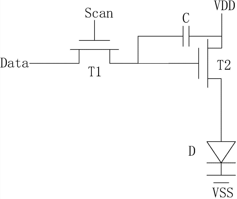
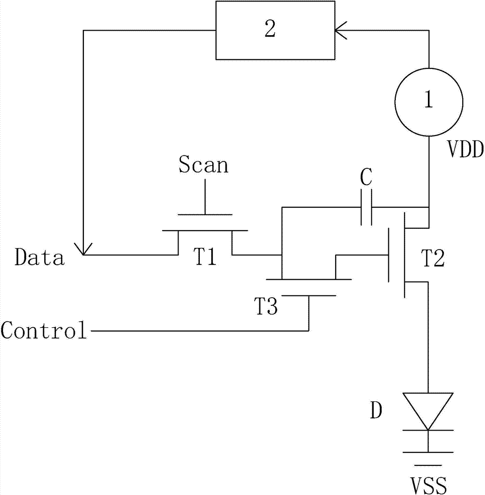
[0032] see figure 2 , the present invention provides an AMOLED pixel circuit, comprising:
[0033] The first thin film transistor T1, the gate of the first thin film transistor T1 is electrically connected to the scan line Scan, the source is electrically connected to the signal line Data, the drain is electrically connected to the source of the third thin film transistor T3, and One end of capacitor C;
[0034] The third thin film transistor T3, the gate of the third thin film transistor T3 is electrically connected to the control line Control, the source is electrically connected to the drain of the first thin film transistor T1, and the drain is electrically connected to the second thin film transistor T2 grid;
[0035] The second thin ...
PUM
 Abstract
Description
Claims
Application Information