

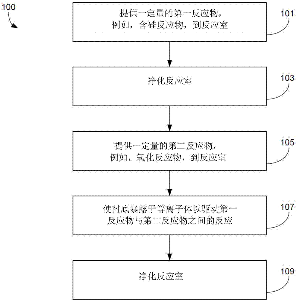
Gapfill of variable aspect ratio features with a composite PEALD and PECVD method
A gap and filling material technology, applied in the direction of coating, gaseous chemical plating, metal material coating process, etc., can solve problems such as inappropriate
- Summary
- Abstract
- Description
- Claims
- Application Information
AI Technical Summary
Problems solved by technology
Method used
Image

Examples
Embodiment Construction
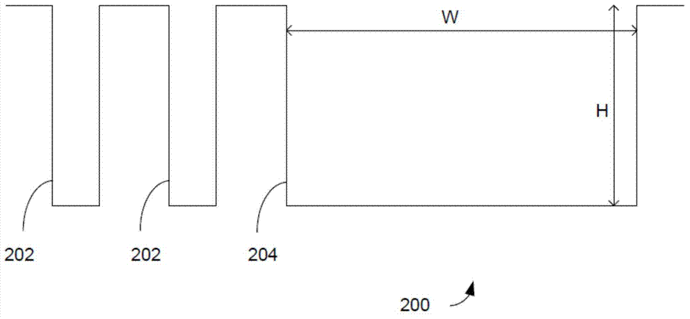
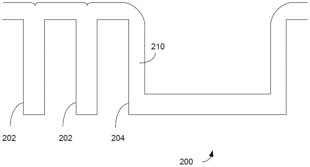
[0027] In this application, the terms "semiconductor wafer", "wafer", "substrate", "wafer substrate" and "partially fabricated integrated circuit" are used interchangeably. Those of ordinary skill in the art will appreciate that a "partially fabricated integrated circuit" may refer to a silicon wafer during any of the many integrated circuit fabrications performed on the silicon wafer. Wafers or substrates used in the semiconductor device industry may have a diameter of 200mm or 300mm or 450mm. The following detailed description assumes that the invention is implemented on a wafer. However, the present invention is not limited thereto. Workpieces can be of many shapes, sizes and materials. In addition to semiconductor wafers, other workpieces that can take advantage of the present invention include various articles such as printed circuit boards, glass panels, and the like.
[0028] In the following description, numerous specific details are set forth in order to provide a ...
PUM
| Property | Measurement | Unit |
|---|---|---|
| Size | aaaaa | aaaaa |
| Size | aaaaa | aaaaa |
Abstract
Description
Claims
Application Information