Barrier film, manufacturing method thereof and display device

A manufacturing method and technology of a display device, which are applied in the manufacture of semiconductor/solid state devices, semiconductor devices, electrical components, etc., can solve problems such as fracture of inorganic layers

Active Publication Date: 2015-04-22
SHANGHAI TIANMA MICRO ELECTRONICS CO LTD +1
View PDF6 Cites 61 Cited by
  • Summary
  • Abstract
  • Description
  • Claims
  • Application Information

AI Technical Summary

Problems solved by technology

[0004] Embodiments of the present invention provide a barrier film, its manufacturing method, and a display device, which are used to solve the techn...

Method used


Image

  • Barrier film, manufacturing method thereof and display device
  • Barrier film, manufacturing method thereof and display device
  • Barrier film, manufacturing method thereof and display device

Examples


Embodiment 1

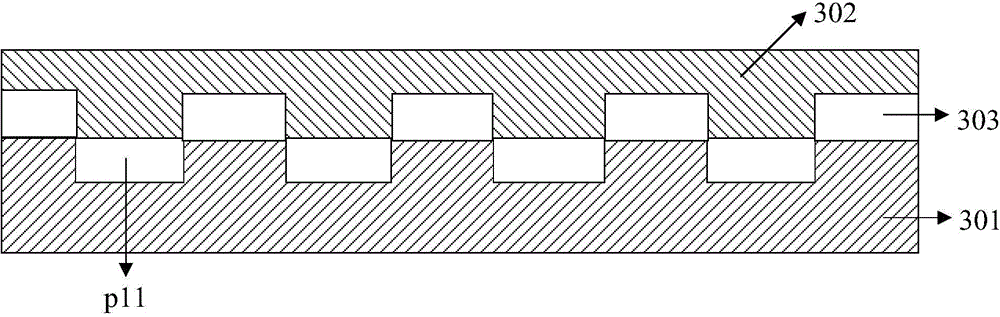
[0022] An embodiment of the present invention provides a barrier film, the barrier film includes a first organic film layer and a second organic film layer, the first organic film layer is formed with a first groove, and the first organic film layer is provided with There is at least one inorganic film layer, the inorganic film layer fills the first groove, and the thickness of the inorganic film layer is less than or equal to the depth of the first groove; the inorganic film layer is provided with the A second organic film layer, the second organic film layer is a planarization layer.

[0023] Specifically, such as image 3 as shown, image 3 A schematic diagram of a barrier film provided in Embodiment 1 of the present invention, the barrier film includes a first organic film layer 301, a second organic film layer 302, and an inorganic film layer 303, and the first organic film layer 301 is formed with a first groove p31 , the inorganic film layer 303 disposed on the first ...

Embodiment 2

[0026] Figure 4 It is a schematic diagram of a barrier film provided in Embodiment 2 of the present invention. The barrier film includes a first organic film layer 401, a second organic film layer 402, an inorganic film layer 403 and an organic film layer 404; the first organic film layer 401 is formed with a first groove p41, which is arranged on the first organic film layer 401 The inorganic film layer 403 on the top fills the first groove p41, and the thickness of the inorganic film layer 403 is less than or equal to the depth of the first groove p41; the organic film layer 404 and the inorganic film layer 403 are alternately stacked at intervals, and the layers of the inorganic film layer 403 The number is at least two layers, the first organic film layer 401 is adjacent to the inorganic film layer 403 arranged thereon, the second organic film layer 402 is adjacent to the inorganic film layer 403 stacked on the organic film layer 404, and the second The organic film laye...

Embodiment 3

[0037] Embodiment 3 of the present invention provides a display device, including a flexible substrate and a light-emitting device disposed on the flexible substrate, the flexible substrate includes a first surface and a second surface oppositely arranged, and the light-emitting device is disposed on the flexible substrate. On the first surface, a first thin film is disposed on the light emitting device, and the first thin film includes the barrier film described in the above embodiments.

[0038] Such as Figure 7 As shown, it is a schematic diagram of a display device provided by Embodiment 3 of the present invention. The display device includes a flexible substrate 701 and a light emitting device 702 disposed on the flexible substrate 701. The light emitting device 702 in the embodiment of the present invention is an OLED device, and the flexible The substrate 701 includes a first surface and a second surface opposite to each other. The light emitting device 702 is disposed...


PUM


Abstract

The embodiment of the invention discloses a barrier film, a manufacturing method thereof and a display device. The barrier film comprises a first organic film layer and a second organic film layer, a first groove is formed in the first organic film layer, at least one inorganic film layer is arranged on the first organic film layer, the first groove is filled with the inorganic film layer, and the thickness of the inorganic film layer is smaller than or equal to the depth of the first groove; the second organic film layer is arranged on the inorganic film layer and is a flattened layer. Due to the fact that the thickness of the inorganic film layer is smaller than or equal to the depth of the first groove, an inorganic layer is discontinuous and does not located in the same layer, the phenomenon of stress concentration can be avoided in the bending process, and the risk that the inorganic layer is cracked is lowered.

Description

technical field [0001] The present invention relates to the field of display technology, in particular to a barrier film and a manufacturing method thereof, and a display device including the barrier film. Background technique [0002] OLED (Organic Light-Emitting Diode, organic light-emitting diode) devices are more and more applied in the display field. The active metal used to form the metal cathode of OLED devices is easy to react with water vapor and oxygen in the air, affecting the injection of charges, and the infiltrated water vapor and oxygen will also chemically react with organic materials, resulting in a decline in the performance of OLED devices. For flexible displays made of soft materials, the barrier film used is usually a laminated structure made of organic and inorganic layers, and the barrier film is encapsulated on the OLED device to prevent moisture and oxygen from interacting with metals. reaction. [0003] However, since the flexible display device i...

Claims


Application Information

Patent Timeline
IPC IPC(8): H01L27/32H01L51/52H01L51/56
Inventor 蔡雨陈正忠
Owner SHANGHAI TIANMA MICRO ELECTRONICS CO LTD
Why Eureka
Try Eureka