Delay compensation method and system of copper plating thickness

A time-delay compensation and electroplating copper technology, which is applied in the direction of circuits, electrolytic components, electrolytic processes, etc., can solve the problems of uncontrollable changes, thickness of electroplating copper layer, thickness of electroplating copper layer, etc.

Active Publication Date: 2015-04-29
HUIZHOU TECHUANG ELECTRONIC TECH CO LTD
View PDF6 Cites 11 Cited by
  • Summary
  • Abstract
  • Description
  • Claims
  • Application Information

AI Technical Summary

Problems solved by technology

[0006] However, the electroplating time required to determine the thickness of the electroplated copper layer through the above-mentioned traditional method still has the following disadvantages: the thickness of the electroplated copper layer obtained in each time period according to the above-mentioned control experiment will vary with the change of the copper plating conditions in the copper plating cylinder , and the changes of these conditions are often uncontrollable, which will cause the thickness of the desired electroplated copper layer to be inconsistent with the actual thickness of the electroplated copper layer

Method used


Image

  • Delay compensation method and system of copper plating thickness
  • Delay compensation method and system of copper plating thickness
  • Delay compensation method and system of copper plating thickness

Examples


Embodiment Construction

[0076] In order to make the above objects, features and advantages of the present invention more comprehensible, specific implementations of the present invention will be described in detail below in conjunction with the accompanying drawings. In the following description, numerous specific details are set forth in order to provide a thorough understanding of the present invention. However, the present invention can be implemented in many other ways different from those described here, and those skilled in the art can make similar improvements without departing from the connotation of the present invention, so the present invention is not limited by the specific implementations disclosed below.

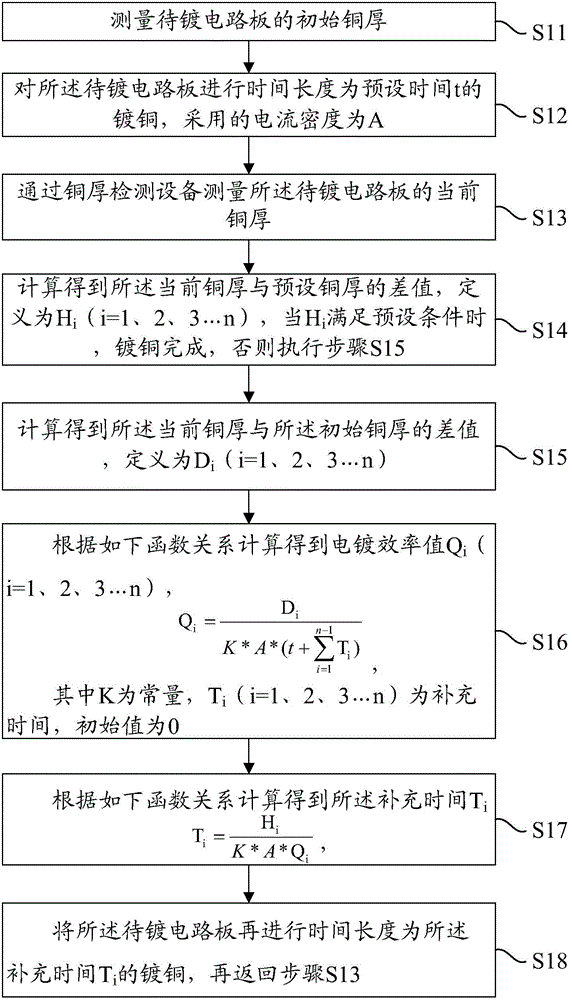
[0077] Such as figure 1 As shown, it is a flow chart of the steps of the delay compensation method for electroplating copper thickness according to an embodiment of the present invention, including the following steps:

[0078] Step S11, measuring the initial copper thickness of the ...


PUM


Abstract

The invention discloses a delay compensation method and system of copper plating thickness, wherein the method comprises the following steps: measuring the initial copper thickness of a circuit board to be plated; plating copper on the circuit board to be plated for preset time t; measuring the current copper thickness of the circuit board to be plated by copper thickness detection equipment; calculating a difference value Hi between the current copper thickness and the preset copper thickness, finishing plating copper when Hi meets preset conditions, or else, continuing to compensate copper plating for time Ti; calculating a difference value Di between the current copper thickness and the initial copper thickness; calculating a plating efficiency value Qi; calculating the compensation time Ti; plating copper on the circuit board to be plated for the compensation time Ti. According to the delay compensation method of copper plating thickness, the compensation time Ti is calculated by modifying and calculating the plating efficiency value Qi, and the copper plating is performed on the circuit board to be plated for the compensation time Ti, so that the thickness of a copper plated layer is more accurate and controllable.

Description

technical field [0001] The invention relates to the field of circuit board electroplating, in particular to a delay compensation method and system for electroplating copper thickness. Background technique [0002] In the circuit board industry, the preparation process of circuit boards mainly includes the following processes: copper clad laminate cutting, drilling and cleaning in holes, pasting photosensitive film, exposure, development, etching, film removal, stacking, lamination, drilling, cleaning and drilling Dirt and copper plating. [0003] The role of the copper plating process is to attach or thicken the copper layer in the drilled hole and on the surface of the circuit. Among them, the copper plating process includes two processes before and after electroless copper plating and electrolytic copper plating. Before electrolytic copper plating, electroless copper plating must first form a conductive layer on the surface of the circuit board, that is, an electroless c...

Claims


Application Information

Patent Timeline
Patent Type & Authority Applications(China)
IPC IPC(8): C25D7/12C25D3/38C25D21/12
Inventor 黄双双
Owner HUIZHOU TECHUANG ELECTRONIC TECH CO LTD
Why Eureka
Try Eureka