Silicon-based waveguide-improved silicon dioxide-based array waveguide grating device and manufacturing method thereof
An arrayed waveguide grating, silica-based technology, applied in the direction of optical waveguide light guide, light guide, optics, etc., can solve problems such as poor wavelength resolution
- Summary
- Abstract
- Description
- Claims
- Application Information
AI Technical Summary
Problems solved by technology
Method used
Image


Examples
Embodiment Construction
[0077] The present invention will be further described below in conjunction with drawings and embodiments.
[0078] The basic idea of the invention is to improve the silicon dioxide-based arrayed waveguide grating by using the silicon-based waveguide to realize the optimization of the wavelength resolution performance.
[0079] 1. Fabrication of silicon dioxide-based arrayed waveguide gratings improved by using silicon-based waveguides
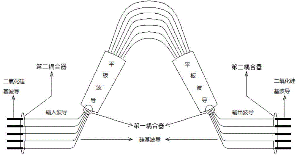
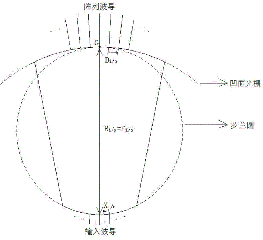
[0080] use as figure 1 or figure 2 As shown in the scheme, a silicon dioxide-based arrayed waveguide grating improved by using a silicon-based waveguide is fabricated.
[0081] use as Figure 5 Processed silicon wafer of the shown cross-section, where the portion used to make the silica-based waveguide is processed as Figure 5 The structure on the left is used to make the silicon-based waveguide part processed as Figure 5 structure on the right.
[0082] exist Figure 5 The silica-based slab waveguide, the silica-based array waveg...
PUM
 Abstract
Description
Claims
Application Information
 - R&D
- Intellectual Property
- Life Sciences
- Materials
- Tech Scout
- Unparalleled Data Quality
- Higher Quality Content
- 60% Fewer Hallucinations
Browse by: Latest US Patents, China's latest patents, Technical Efficacy Thesaurus, Application Domain, Technology Topic, Popular Technical Reports.
© 2025 PatSnap. All rights reserved.Legal|Privacy policy|Modern Slavery Act Transparency Statement|Sitemap|About US| Contact US: help@patsnap.com