An Optical and Digital Joint Design Method for Digital Imaging System

A technology of a digital imaging system and design method, applied in optics, optical components, instruments, etc., can solve the problems of lens processing, adjustment, detection difficulties, long research and development cycle, and large volume and weight of imaging systems.

Active Publication Date: 2017-02-22
ACAD OF OPTO ELECTRONICS CHINESE ACAD OF SCI
View PDF3 Cites 0 Cited by
  • Summary
  • Abstract
  • Description
  • Claims
  • Application Information

AI Technical Summary

Problems solved by technology

[0004] The traditional design method makes the quality of the optical system design the only link that determines the image quality. In order to "perfectly" correct the aberration, the optical lens usually needs to be composed of multiple lenses, and the curvature of the lens may also be aspherical, which leads to lens processing, assembly, etc. It is extremely difficult to adjust and detect, which makes the imaging system large in size and weight, long in development cycle, and high in cost
However, no matter how many lenses there are and how complex the curvature is, it is far less than the number of various order aberrations. Each aberration will still have a certain amount of residue, which will affect the clarity of the image.
In addition, although the digital processing method of sharpening to improve contrast and smoothing to improve the signal-to-noise ratio can be used to improve the image clarity, the improvement of the signal-to-noise ratio and the improvement of the contrast are mutually restricted, and it is difficult to take care of each other. Adding the average will inevitably reduce the contrast, and the introduction of convolution algorithm for image sharpening will inevitably amplify the noise or introduce new noise

Method used


Image

  • An Optical and Digital Joint Design Method for Digital Imaging System
  • An Optical and Digital Joint Design Method for Digital Imaging System
  • An Optical and Digital Joint Design Method for Digital Imaging System

Examples


Embodiment Construction

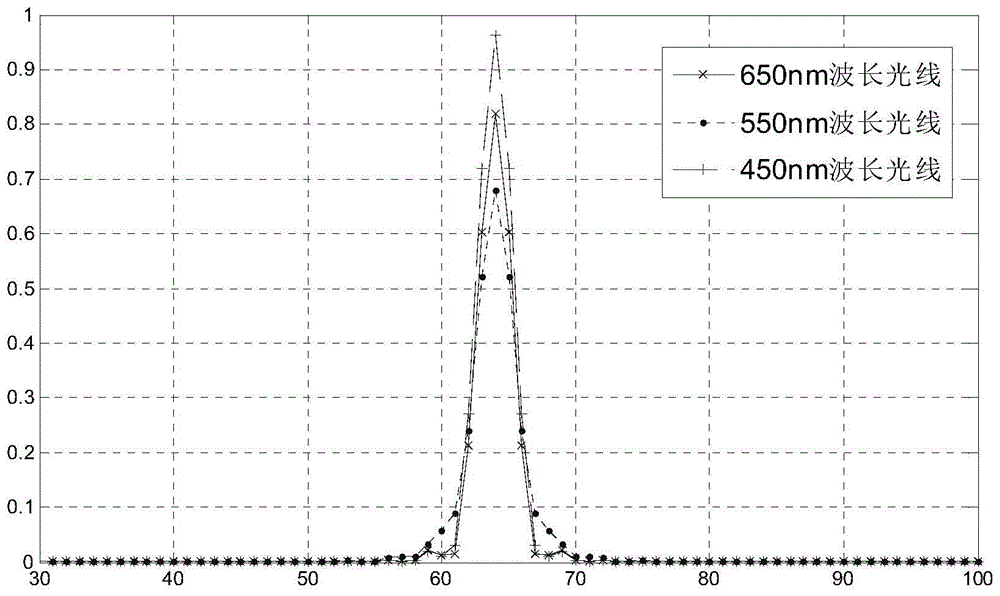
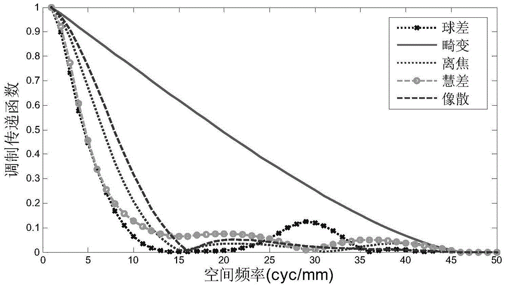
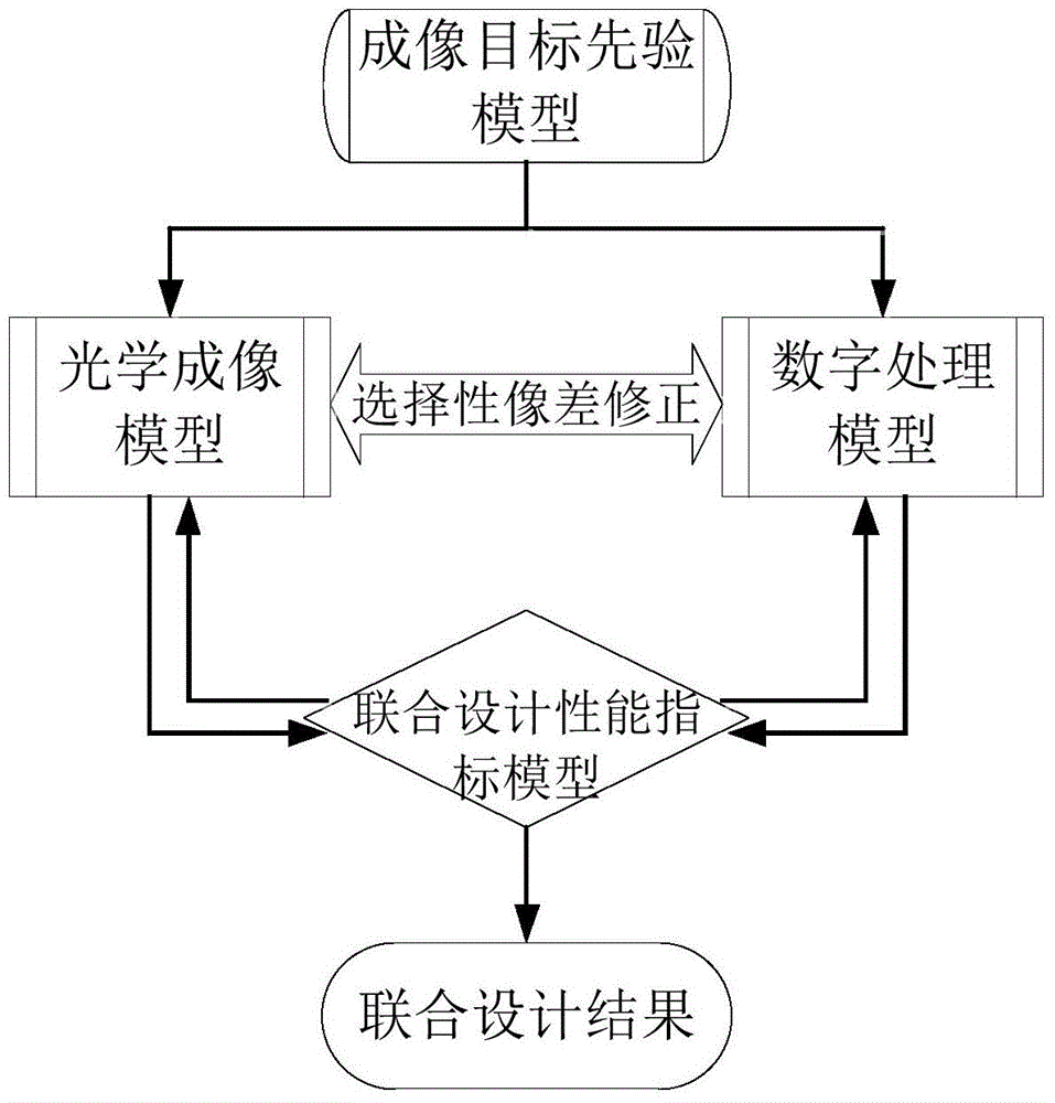
[0073] The technical key point of the present invention is to analyze the difficulty of using digital processing to compensate for chromatic aberration, defocus, distortion, astigmatism, coma, curvature of field, and spherical aberration. The aberration is left to the optical design correction, the aberration that is easy to be compensated by digital processing is corrected by the image processing algorithm, and the digital is realized by modeling the prior information of the imaging target, the optical imaging system, the digital processing system, and the performance index of the joint design. The optical / digital joint design of the imaging system relaxes the strict restrictions on the optical system, reduces the complexity of the optical system, and at the same time realizes the global optimization of optical design and digital processing.

[0074] Such as image 3 As shown, the specific implementation steps of the optical and digital joint design method of the digital imaging...


PUM


Abstract

The invention relates to an optical and digital combined design method of a digital imaging system. The method comprises the steps that by analyzing the difficulty degree of digitally processing imaging definition losses caused by compensation of chromatic aberration, out-of-focus, distortion, astigmatism, coma, curvature of the field and spherical aberration, aberration difficult to compensate for through digital processing is corrected through optical design, and aberration easy to compensate for through digital processing is corrected through an image processing algorithm; optical and digital combined iterative optimization design of the digital imaging system is achieved by modeling imaging target prior information, an optical imaging system, a digital processing system and combined design performance indexes. In this way, strict restriction on the optical system is relaxed, the complexity of the optical system is lowered, and global optimization of optical design and digital processing is achieved.

Description

Technical field [0001] The invention relates to an optical and digital joint design method of a digital imaging system. Background technique [0002] With the rapid development of electronic technology and material technology, the imaging system has been developed from silver halide film imaging to digital imaging. Now the traditional digital imaging system is mainly composed of an optical system and a detector system. The target is imaged on the CCD or The digital image is formed on the COMS detector, and people use image processing algorithms to more or less modify the digital image according to the application needs. Digital image processing is not an essential part of the traditional digital imaging system. In this way, In a certain sense, the characteristics of so-called "digital" imaging have been lost, and all the advantages of digital imaging have not been fully exploited. [0003] The traditional digital imaging system design method is mainly divided into two steps: The f...

Claims


Application Information

Patent Timeline
Patent Type & Authority Patents(China)
IPC IPC(8): G02B27/00
CPCG02B27/0012
Inventor 相里斌张金刚谭政方煜吕群波杜述松付强孙建颖白杨丛林骁
Owner ACAD OF OPTO ELECTRONICS CHINESE ACAD OF SCI
Why Eureka
Try Eureka