Layout Method of Meshless Analog Circuit Based on Split Block

A technology of analog circuit and wiring method, which is applied in the direction of electrical digital data processing, special data processing applications, instruments, etc., to achieve the effects of reducing time, reducing the number of searches, and increasing accuracy

Inactive Publication Date: 2018-03-02
WUHAN UNIV OF TECH
View PDF5 Cites 0 Cited by
  • Summary
  • Abstract
  • Description
  • Claims
  • Application Information

AI Technical Summary

Problems solved by technology

However, since the grid size in grid wiring is uniform, it is generally only applicable to the case of uniform line width in analog circuits.

Method used


Image

  • Layout Method of Meshless Analog Circuit Based on Split Block
  • Layout Method of Meshless Analog Circuit Based on Split Block
  • Layout Method of Meshless Analog Circuit Based on Split Block

Examples


Embodiment Construction

[0039] The present invention will be further described in detail below in conjunction with the accompanying drawings and specific embodiments.

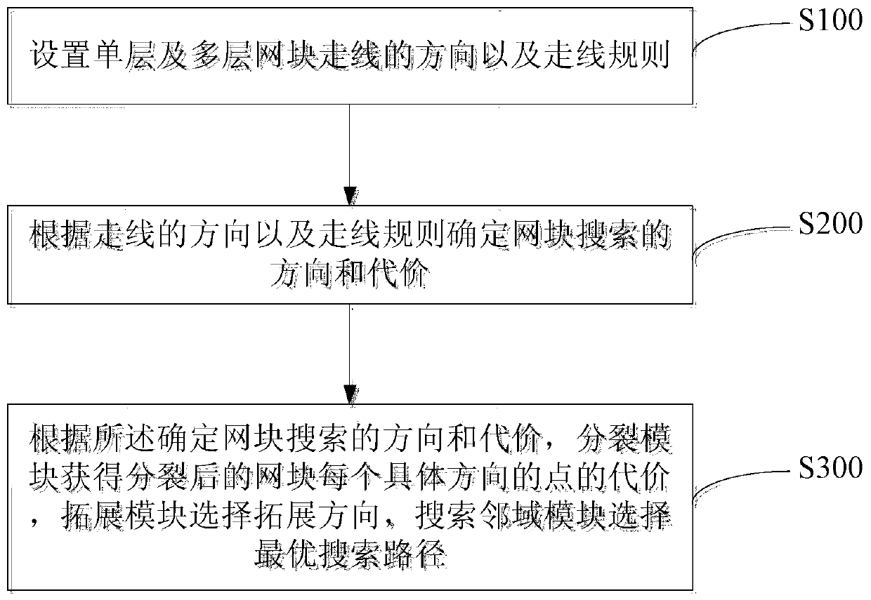
[0040] Such as figure 1 As shown, the wiring method of the gridless analog circuit based on the split block of the present invention comprises:

[0041] S100, setting the routing direction and routing rules of single-layer and multi-layer network blocks.

[0042] S200. Determine the direction and cost of network block search according to the routing direction and routing rules.

[0043] S300. According to the determination of the search direction and cost of the network block, the splitting module obtains the cost of points in each specific direction of the split network block, the expansion module selects the expansion direction, and the search neighborhood module selects the optimal search path.

[0044] In the above steps, specifically include:

[0045] 1. Build a search model

[0046] Before wiring, it is first necessary to de...


PUM


Abstract

The invention relates to a wiring method of a split block-based mesh-less analog circuit. The method comprises the steps of setting cabling directions and cabling rules of single layer or multi-layer net grids; determining the searching direction and price of the net grids in accordance with the cabling direction and cabling rules; obtaining the point of each specific direction of the net grid split by the split module in accordance with the direction and price for searching the net grids, expanding a module selection expanding direction and searching an optimum searching route of a module in a neighbor-hood. According to the wiring method provided by the invention, the modules can be found out efficiently, and correct wiring can be realized, therefore, the wiring method has an important meaning in the course of guiding wiring optimization and detailed wiring process.

Description

technical field [0001] The invention relates to a wiring model of a gridless analog circuit, in particular to a wiring method of a gridless analog circuit based on split blocks. Background technique [0002] Since the invention of the first transistor in the 1950s, the manufacturing process of integrated circuits has developed rapidly. The semiconductor processing technology has entered the nanometer era, the integration scale has reached a very large scale, and the functions have become more and more diversified, making it possible to integrate digital circuits and analog circuits on a chip. . The digital circuit and its automatic design technology have matured day by day, which can realize large-scale and highly complex layout automatic design. However, the diversified requirements of integrated circuit functions make the mixed circuits of analog circuits and digital circuits account for an increasing proportion in SoCs. Since the analog circuit is very different from t...

Claims


Application Information

Patent Timeline
Patent Type & Authority Patents(China)
IPC IPC(8): G06F17/50
Inventor 徐宁于本志余姣姣
Owner WUHAN UNIV OF TECH
Why Eureka
Try Eureka