Apparatus and method for manufacturing electronic component

A technology for electronic components and manufacturing equipment, which is applied in the manufacture of semiconductor/solid-state devices, electrical components, circuits, etc., can solve the problems of electronic components 29 falling, unoptimized, static electricity, etc., to reduce the installation area, improve the operation rate, and improve the The effect of yield

Active Publication Date: 2015-04-29
TOWA
View PDF4 Cites 2 Cited by
  • Summary
  • Abstract
  • Description
  • Claims
  • Application Information

AI Technical Summary

Problems solved by technology

First, due to the cutting water, there may be a situation where the electronic components 29 that are closely attached to the lower surface of the first conveying mechanism 8 do not fall.
Second, in the case where the first conveying mechanism 8 is formed of a rubber-based material (for example, refer to Patent Document 2) in order to facilitate the formation of the recess 25 and the suction path 26, since the electronic component 29 is easily adhered to the surface of the first conveying mechanism 8 The lower surface may produce the situation that the electronic component 29 does not fall from the lower surface of the first transport mechanism 8
However, this method increases the installation area (occupancy area) of the manufacturing apparatus M2 of the electronic component, so it is not preferable.
[0026] The second problem is as follows: the electronic component 29 is caught between the wires 35 of the brush, so that the electronic component 29 cannot be accommodated inside the storage box 33
However, this method reduces the operation rate of the electronic component manufacturing apparatus M2, so it is not preferable.
[0027] The third problem is as follows: When the wire 35 of the brush and the electronic part 29 are separated after being in contact, static electricity is generated, and this static electricity has a bad influence on the electronic part 29
Therefore, depending on the type of electronic component 29, the yield of electronic component 29 may decrease due to static electricity.

Method used


Image

  • Apparatus and method for manufacturing electronic component
  • Apparatus and method for manufacturing electronic component
  • Apparatus and method for manufacturing electronic component

Examples


Embodiment 1

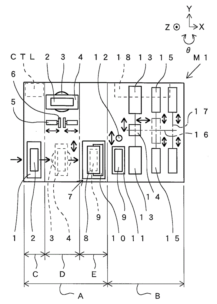
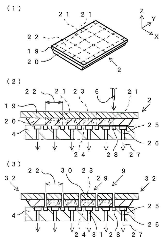
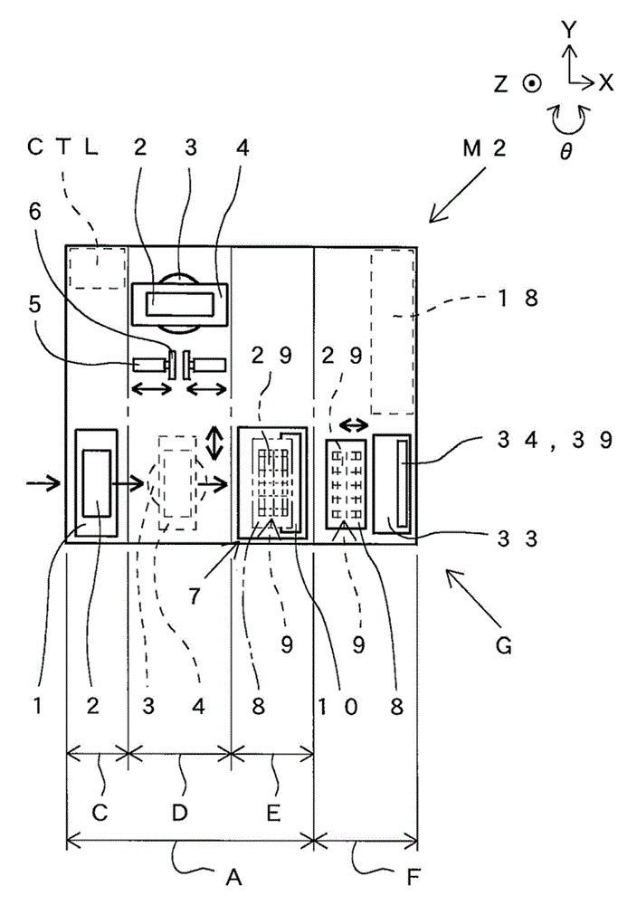
[0119] refer to image 3 with Figure 5 , Example 1 of the manufacturing apparatus M2 and the manufacturing method of the electronic component 29 using the manufacturing apparatus M2 will be described. Such as Figure 5 As shown, the scraping member 39 used in this embodiment is composed of a rigid member. More specifically, the scraping member 39 has a plurality of rod-shaped members 40 having rigidity. The rod member 40 has a cylindrical shape. The intervals between the plurality of bar-shaped members 40 are preferably smaller than the minimum size of the electronic component 29 (generally, the dimension in the thickness direction (Z direction in the figure)). In addition, regarding this case, that is, when it is preferable that the interval between a plurality of components (in this embodiment, a plurality of rod-shaped components 40 ) is smaller than the minimum value of the size of the electronic component 29, in other implementations described later, The same applie...

Embodiment 2

[0127] refer to image 3 and Figure 6 , Example 2 of the manufacturing apparatus M2 and the electronic component 29 using the manufacturing apparatus M2 will be described. Such as Figure 6 As shown, the scraping member 39 used in this embodiment has a single plate-shaped member 41 composed of a rigid member.

[0128] The single plate member 41 included in the scraping member 39 scrapes off the plurality of electronic components 29 from the first conveying mechanism 8 by the movement of the first conveying mechanism 8 . The scraped-off electronic components 29 are housed in the storage box 29 .

[0129] According to this embodiment, the same effect as that of the embodiment described above can be obtained. In particular, since the scraping member 39 having the single plate-like member 41 is used, the phenomenon that the electronic part 29 is caught in the scraping member 39 never occurs. Therefore, since the electronic component 29 is reliably accommodated in the storage...

Embodiment 3

[0131] refer to image 3 and Figure 7 , Example 3 of the manufacturing apparatus M2 and the electronic component 29 using the manufacturing apparatus M2 will be described. Such as Figure 7 As shown, in this embodiment, a switching valve 42 is provided on the suction pipe 36 connected to the suction pump 18 . The switching valve 42 and the suction pump 18 are connected through the suction pipe 36 . The switching valve 42 and a high-pressure gas source (not shown) are connected through a pipe 43 for injection. In the present embodiment, the suction duct 36 between the switching valve 42 and the first transport mechanism 8 also functions as an injection duct. As the high-pressure gas source, a high-pressure air source that is utility equipment (Utilities) in an electronic component manufacturing plant can be used.

[0132] Next, the operation of the manufacturing apparatus of this embodiment will be described. First, the suction pump 18 and the suction pipe 36 are connect...


PUM


Abstract

The invention provides an apparatus and a method for manufacturing an electronic component. According to the apparatus and the method, a plurality of electronic parts are exactly contained at the inner part of a container by the cutting of cut objects. A packaging substrate provided with an integral substrate and semiconductor chips is cut to a plurality of area units to manufacture the plurality of electronic parts, the apparatus for manufacturing the electronic component comprises a rotation blade, a first conveying mechanism for fixing and moving the plurality of electronic parts, an output portion for outputting the plurality of electronic parts to the outside of the manufacturing apparatus, the container arranged below a moving path of the first conveying mechanism, and a scraping part fixed at the inner side of the container and is formed by a single plate-shaped part as a rigid part, wherein the integral substrate is provided with a plurality of areas, and the semiconductor chips are respectively arranged in the plurality of areas. By the movement of the first conveying mechanism, the scraping part and the electronic parts are contacted, the electronic parts are scraped, and the scraped electronic parts are contained in the container.

Description

technical field [0001] The present invention relates to an electronic component manufacturing apparatus and method for manufacturing a plurality of electronic components by cutting a cut object having at least a monolithic substrate and a functional portion, wherein the monolithic substrate has a plurality of regions, and The functional parts described above exist in the plurality of regions and function as electronic devices. Background technique [0002] When manufacturing electronic components, a technique of singulation into a plurality of electronic components by cutting a resin package using a rotating blade (blade) is widely practiced (for example, refer to Patent Document 1). [0003] refer to figure 1 , a first conventional example of a manufacturing apparatus of an electronic component will be described. figure 1 It is a plan view which shows the 1st conventional example of the manufacturing apparatus of an electronic component. In addition, for the convenience ...

Claims


Application Information

Patent Timeline
Patent Type & Authority Applications(China)
IPC IPC(8): H01L21/301H01L21/78
CPCH01L21/304H01L21/30625H01L21/677H01L21/78
Inventor 和泉裕也新田一法吉见裕子石桥干司
Owner TOWA
Why Eureka
Try Eureka