Manufacturing method of burn-in semiconductor test board

A burn-in and manufacturing method technology, applied in the direction of semiconductor/solid-state device testing/measurement, etc., can solve problems such as difficulty in ensuring alignment requirements, scratched board surface, and substandard board thickness in the gold finger area, so as to improve good quality, Design optimization and the effect of solving the problem of substandard plate thickness

Inactive Publication Date: 2017-11-17
GUANGZHOU FASTPRINT CIRCUIT TECH +2
View PDF3 Cites 0 Cited by
  • Summary
  • Abstract
  • Description
  • Claims
  • Application Information

AI Technical Summary

Problems solved by technology

In the existing technology, due to the characteristics of the Burn-in semiconductor test board, the difficulties in its production are mainly reflected in the following: First, the problem of the size of the ultra-long board: in the transfer process after the outer graphics process, scratches are prone to occur Or the problem of the graphic on the scratched board surface, and there is no protective measure for the graphic on the board surface in the post-processing process
Second, the problems in the gold finger area: the inner layer design of the gold finger area of ​​the burn-in semiconductor test board is generally the base material, and the existing method for designing the thickness of the laminated structure is: lamination design plate thickness range = complete Board thickness range - thickness range of outer copper plating layer - thickness range of solder mask layer, this laminated structure can easily lead to substandard board thickness in the gold finger area, thicker or thinner, and the common process edge, that is, flow block or Choke point, see figure 2 and image 3 , during the lamination process, it is easy to cause the problem of copper foil wrinkling in the gold finger area after lamination
Third, the alignment problem of the array BGA: each BGA unit has a pitch of 0.4mm, and the wiring in the BGA is currently commonly used in the 3-hole or 4-hole positioning drilling method, which is difficult to guarantee 0.4mm For the alignment requirements of the pitch, use the target holes on the edge of the board to measure the expansion and contraction in the X and Y directions, and use it to stretch the drill tapes of all BGAs on the entire board for drilling, and it is impossible to guarantee the alignment of all BGA holes. bit effects
refer to Figure 4 , in the actual production process, due to the bonding of the semi-cured edge of the inner layer of the PCB board, the inner layer graphics of the board will expand and shrink after pressing, and the traditional method of stretching the drill tape is to measure the edge of the board The distance between the 4 targets 30' to calculate the overall expansion and contraction value, that is, 2 in the long direction and 2 in the short direction to measure the overall expansion and contraction value, which is used to stretch the overall drilling belt. This kind of expansion and contraction measurement is not conducive to Small pitch BGA drilling alignment

Method used


Image

  • Manufacturing method of burn-in semiconductor test board
  • Manufacturing method of burn-in semiconductor test board
  • Manufacturing method of burn-in semiconductor test board

Examples


Embodiment Construction

[0025] It should be noted that, in the case of no conflict, the embodiments in the present application and the technical features in the embodiments can be combined with each other. The present invention will be further described in detail below in conjunction with the drawings and specific embodiments.

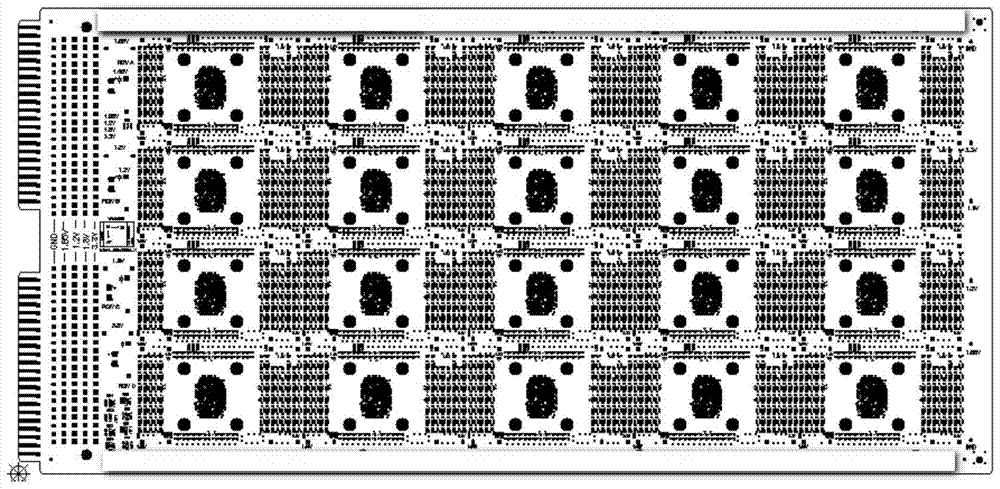
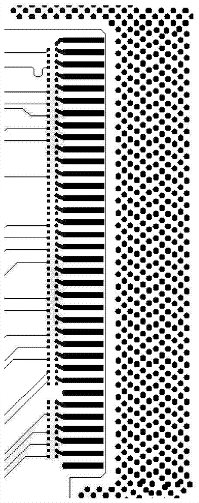
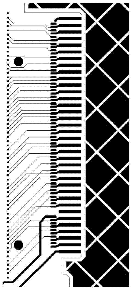
[0026] The present invention is a kind of manufacture method of Burn-in semiconductor test board, refer to Figure 5 to Figure 7 , including the protection step of the BGA area on the test board during the transmission process, the stacking step of the golden finger area on the test board and the manufacturing step of the process edge, and the steps of individually positioning each BGA to measure expansion and contraction and drilling.

[0027] The Burn-in semiconductor test board has an ultra-long board size. The protection steps of the BGA area on the test board include: after the surface treatment of the board body, select a transparent micro-mucosa with the same size as th...


PUM


Abstract

The invention relates to a manufacturing method for a Burn-in semiconductor test board. The manufacturing method includes the procedure of adopting a transparent micro-adhesion film for protecting the BGA region of an ultra-high board size, the thickness method of a lamination structure of a gold finger region, the procedure of manufacturing a technology edge through combination of flow stopping blocks and flow stopping points and the mode of independently measuring expanding and shrinking of each BGA unit of a BGA and drilling of each BGA unit of the BGA through positioning. The problems that the Burn-in semiconductor test board is high in requirement for aligning of the BGA, has the requirement for the thickness of the gold finger board and is prone to wrinkling are solved, and the manufacturing methods of difficult points are optimized so that a higher product yield can be achieved.

Description

technical field [0001] The invention relates to the field of manufacturing semiconductor test boards, in particular to a method for manufacturing a burn-in semiconductor test board. Background technique [0002] As a high value-added PCB board, semiconductor test boards are used to test semiconductor wafers to screen out qualified products. Generally, they can be divided into ATE test boards, probe-card test boards and burn-in test boards. refer to figure 1 , where the burn-in semiconductor test board has an array BGA (4*4 or 5*4) with super long size (long side > 20inch), golden finger, small pitch (0.4mm or 0.5mm, requiring wiring in BGA) ) and the BGA needs to be installed with a socket. At present, the appearance requirements for the scratches of the pad base material of the BGA and the defect of the pad are becoming more and more strict, so the manufacturing of the semiconductor test board is more difficult than the production of ordinary PCB boards. In the existing t...

Claims


Application Information

Patent Timeline
Patent Type & Authority Patents(China)
IPC IPC(8): H01L21/66
Inventor 罗娜史宏宇李艳国
Owner GUANGZHOU FASTPRINT CIRCUIT TECH
Why Eureka
Try Eureka