Array substrate, array substrate manufacturing method and display panel

A technology for array substrates and display areas, applied in semiconductor/solid-state device manufacturing, instruments, semiconductor devices, etc., can solve the problems of narrowing of the frame of the display device, large capacitor length, etc., and achieve the effect of reducing the size of the area and reducing the width

Inactive Publication Date: 2015-05-20
SHANGHAI TIANMA MICRO ELECTRONICS CO LTD +1
View PDF8 Cites 13 Cited by
  • Summary
  • Abstract
  • Description
  • Claims
  • Application Information

AI Technical Summary

Problems solved by technology

However, in order to meet the design specifications of the capacitor, the length of the capacitor usually needs to be made larger, which limits the size of the GOA circuit and makes it difficult to further narrow the frame of the display device.

Method used


Image

  • Array substrate, array substrate manufacturing method and display panel
  • Array substrate, array substrate manufacturing method and display panel
  • Array substrate, array substrate manufacturing method and display panel

Examples


Embodiment Construction

[0014] The following will clearly and completely describe the technical solutions in the embodiments of the present invention with reference to the accompanying drawings in the embodiments of the present invention. Obviously, the described embodiments are only some, not all, embodiments of the present invention. Based on the embodiments of the present invention, all other embodiments obtained by persons of ordinary skill in the art without creative efforts fall within the protection scope of the present invention.

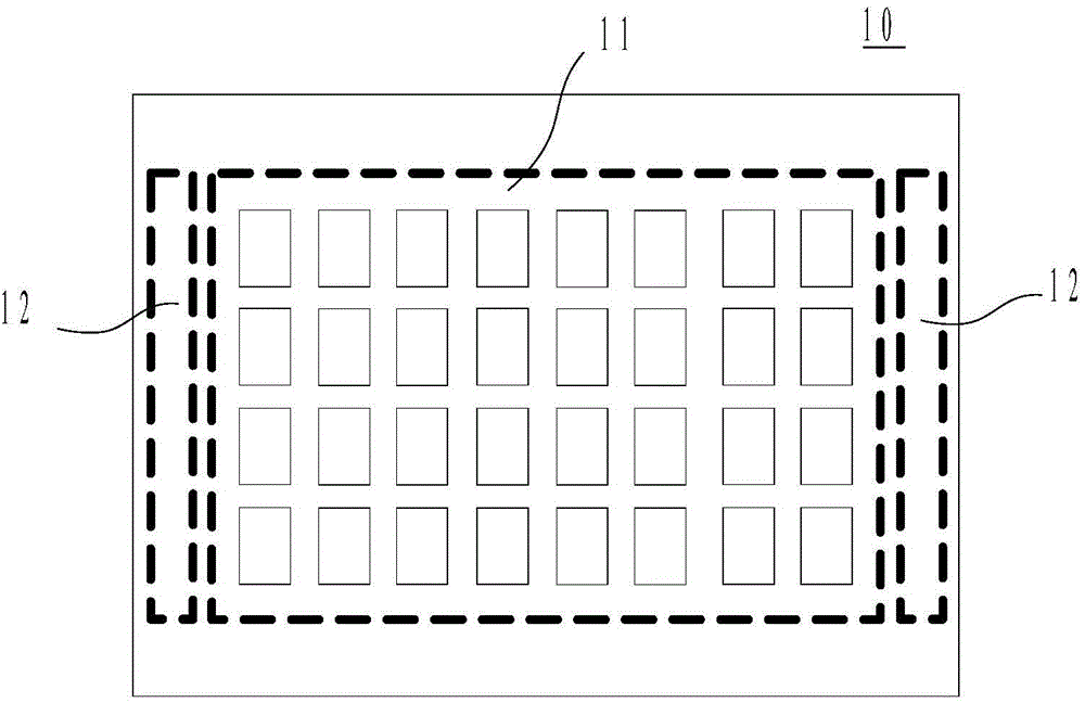
[0015] figure 1 Shown is a top view of an array substrate 10 provided by an embodiment of the present invention. The array substrate 10 includes: a display area 11 and a non-display area (except the peripheral area of ​​the display area 11), wherein the non-display area includes The amorphous silicon gate region 12 for the signal, the amorphous silicon gate region 12 is generally arranged in the non-display regions on the left and right sides of the array substrate...


PUM


Abstract

The invention discloses an array substrate which comprises a display area and a non-display area. The non-display area comprises an amorphous silicon grid area used for outputting grid drive signals. The array substrate is characterized in that the amorphous silicon grid area comprises a first capacitor and a second capacitor, the first capacitor comprises a first polar plate and a second polar plate, the second capacitor comprises a third polar plate and a fourth polar plate, a third capacitor is further included, and the third capacitor is composed of the second polar plate and the third polar plate, wherein the first polar plate is electrically connected with the third polar plate, the second polar plate is electrically connected with the fourth polar plate, and at least part of projections of any two adjacent polar plates of the first polar plate, the second polar plate, the third polar plate and the fourth polar plate are overlapped in the vertical direction of the array substrate.

Description

technical field [0001] The present invention relates to the field of display technology, in particular to an array substrate and a method for manufacturing the array substrate. Background technique [0002] In order to improve the display effect of the display device, more and more people begin to pay attention to the narrow bezel design of the display device, especially for the splicing screen used for large-screen outdoor display, the narrow bezel display device can effectively reduce the splicing in the splicing screen. The width of the seam significantly improves the overall display effect. [0003] In the existing technology, the production of narrow-frame displays is usually achieved by compressing the process margin to the limit. One of the very important technologies is the mass production of the display panel Gate Driver on Array (GOA) technology. accomplish. GOA technology is used to integrate the gate switch circuit on the array substrate to form a scan drive fo...

Claims


Application Information

Patent Timeline
Patent Type & Authority Applications(China)
IPC IPC(8): G02F1/1362G02F1/1368G02F1/1343H01L27/06H01L29/423H01L21/82H01L21/28
CPCG02F1/136213G02F1/133345G02F1/1343G02F1/136227H01L21/28H01L21/82H01L27/06H01L29/423
Inventor 孙云刚杨康李谷骏
Owner SHANGHAI TIANMA MICRO ELECTRONICS CO LTD
Why Eureka
Try Eureka