
A kind of nandflash firmware burning device and burning method

A burning method and burner technology, which are applied in the direction of instruments, software engineering design, electrical digital data processing, etc., can solve the problems of returning to the factory for maintenance and the limited number of chips, so as to reduce the workload, ensure the quality of burning chips, and easily The effect of replacement

Active Publication Date: 2018-02-09
FUJIAN SHIDA COMP EQUIP
View PDF4 Cites 0 Cited by
  • Summary
  • Abstract
  • Description
  • Claims
  • Application Information

AI Technical Summary

Problems solved by technology

Moreover, the SOCKET of a programmer (the seat used to put the components to be processed) not only has a limited number of chips to burn, but also is a consumable. If it is damaged, the whole machine can only be returned to the factory for repair, and the requirements for the operator It is relatively high, so it is increasingly urgent to invent a burner that can operate independently without a computer, is easy to operate, and can expand many independent modules according to needs.

Method used

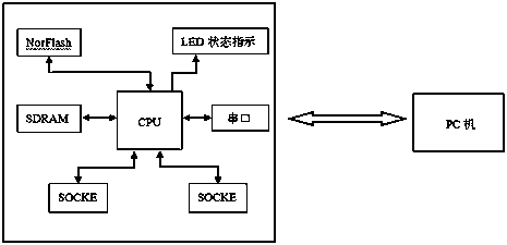
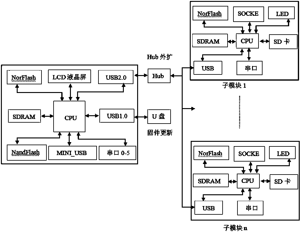
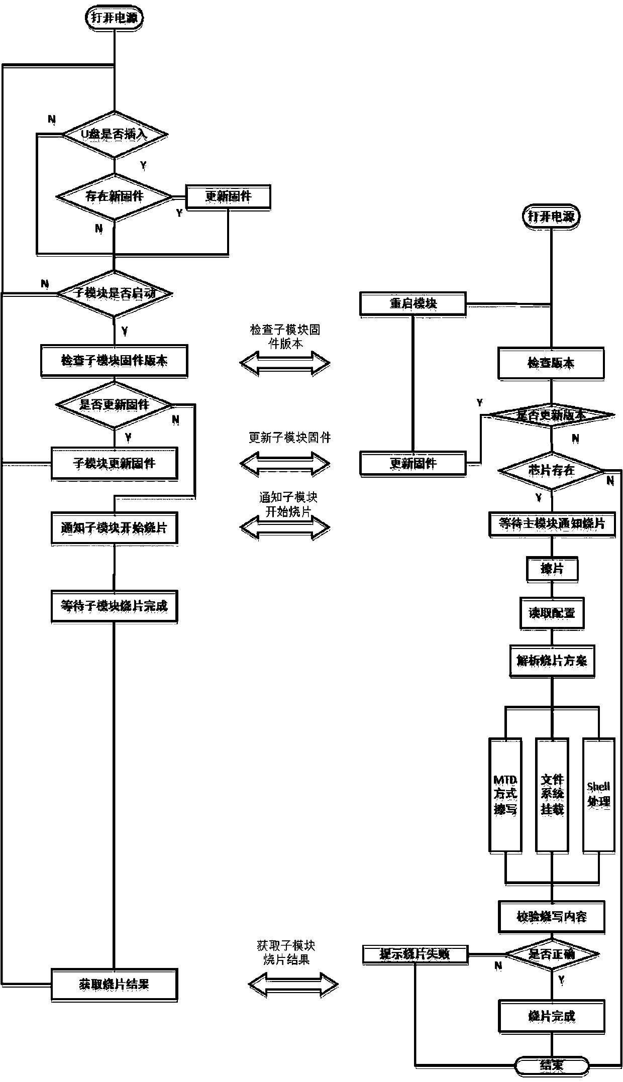

Image

  • A kind of nandflash firmware burning device and burning method
  • A kind of nandflash firmware burning device and burning method
  • A kind of nandflash firmware burning device and burning method

Examples


Embodiment Construction

[0035] In order to make the above objects, features and advantages of the present invention more comprehensible, specific implementations of the present invention will be described in detail below in conjunction with the accompanying drawings.

[0036] In the following description, specific details are set forth in order to provide a thorough understanding of the present invention. However, the present invention can be implemented in many other ways than those described here, and those skilled in the art can make similar extensions without departing from the connotation of the present invention. Accordingly, the present invention is not limited to the specific embodiments disclosed below.

[0037] The burner of the present embodiment is a NandFlash firmware burner based on the Linux file system, and is used to burn batches of firmware to NandFlash chips during the production process. It is controlled by a main module to burn multiple sub-modules that can be expanded. The burn...


PUM


Abstract

The invention relates to a NandFlash firmware programmer and a programming method. The NandFlash firmware programmer and the programming method are used for conducting firmware batch programming on a NandFlash chip in the production process. The programmer comprises a main module and N sub modules. The main module comprises a first CPU, a first SDRAM, a NandFlash, a first NorFlash, a liquid crystal display (LED), a USB 2.0 interface circuit, a USB 1.0 interface circuit, a MINI-USB interface circuit and a first serial interface circuit, wherein the first SDRAM, the NandFlash, the first NorFlash, the liquid crystal display (LED), the USB2.0 interface circuit, the USB 1.0 interface circuit, the MINI-USB interface circuit and the first serial interface circuit are connected with the first CPU. Each sub module comprises a second CPU, a second SDRAM, a second NorFlash, a USB interface circuit, a second serial interface circuit, an LED indicator light and an SOCKET, wherein the second SDRAM, the second NorFlash, the USB interface circuit, the second serial interface circuit, the LED indicator light and the SOCKET are connected with the second CPU. The USB 2.0 interface circuit is connected with the USB interface circuit through a USB HUB device. The NandFlash firmware programmer and the programming method aim to achieve direct chip programming of the NandFlash, support using of multiple kinds of chip programming schemes and achieve file system mounting of NandFlash partition.

Description

technical field [0001] The invention relates to the technical field of device programming, especially based on the Linux platform, and relates to the erasing and writing control of MTD equipment (memorytechnology device), which is mainly used for firmware downloading of large quantities of NandFlash chips in the production process. Background technique [0002] At present, most electronic products use NandFlash as a storage device. Therefore, it is necessary to pre-install the firmware of NandFlash, and the traditional download method is to solder NandFlash to the motherboard and transfer it into a complete machine, and then use the PC to use Samba software to perform ISP (In System Program in-system programming) on ​​the assembled machine. ) firmware download, because the bad blocks in NandFlash are randomly distributed, the chip cannot be scanned for bad blocks before downloading. If it is found that the chip is a defective product when the whole machine is downloaded, th...

Claims


Application Information

Patent Timeline
Patent Type & Authority Patents(China)
IPC IPC(8): G06F8/654G06F13/10
Inventor 陈敏陈先樑黄凌帆黄少斌林洪华
Owner FUJIAN SHIDA COMP EQUIP
Learn More