Workpiece processing device
A processing device and workpiece technology, applied in the direction of electrical components, semiconductor/solid-state device manufacturing, circuits, etc., can solve the problems of inconvenient and flexible, and achieve the effect of improving workpiece processing efficiency, reducing workpiece processing cost, and convenient use
- Summary
- Abstract
- Description
- Claims
- Application Information
AI Technical Summary
Problems solved by technology
Method used
Image

Examples
Embodiment Construction
[0027] In order to describe the technical content, structural features, achieved goals and effects of the present invention in detail, the following will be described in detail in conjunction with the embodiments and accompanying drawings.
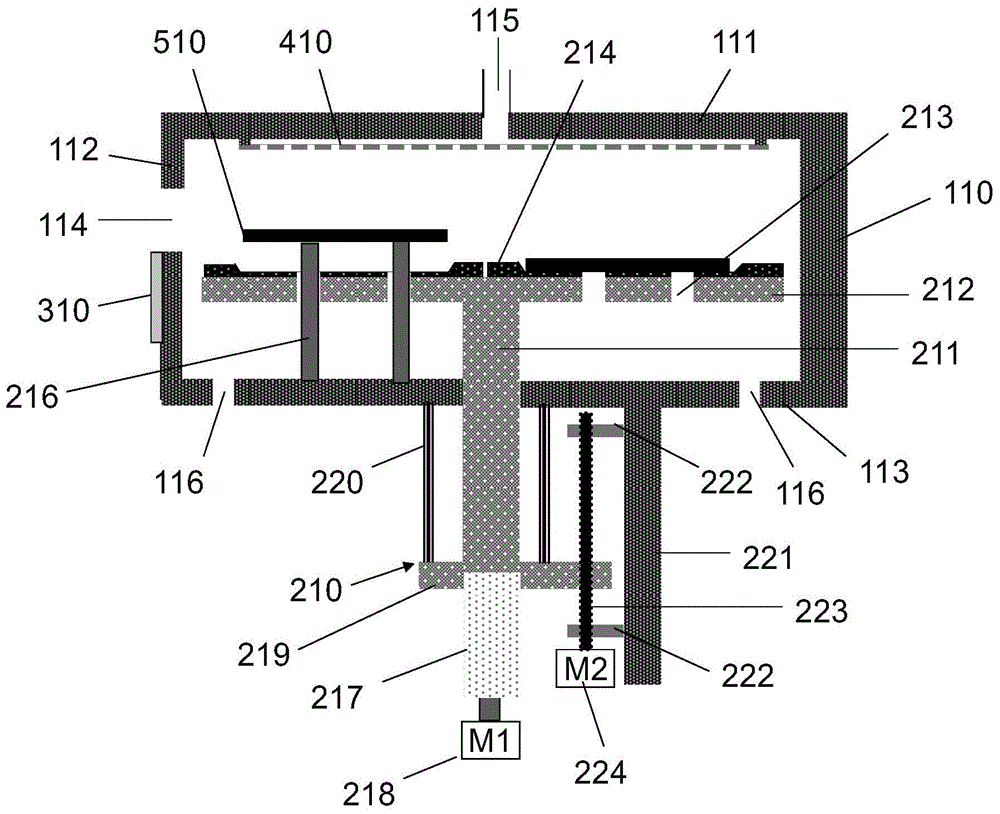
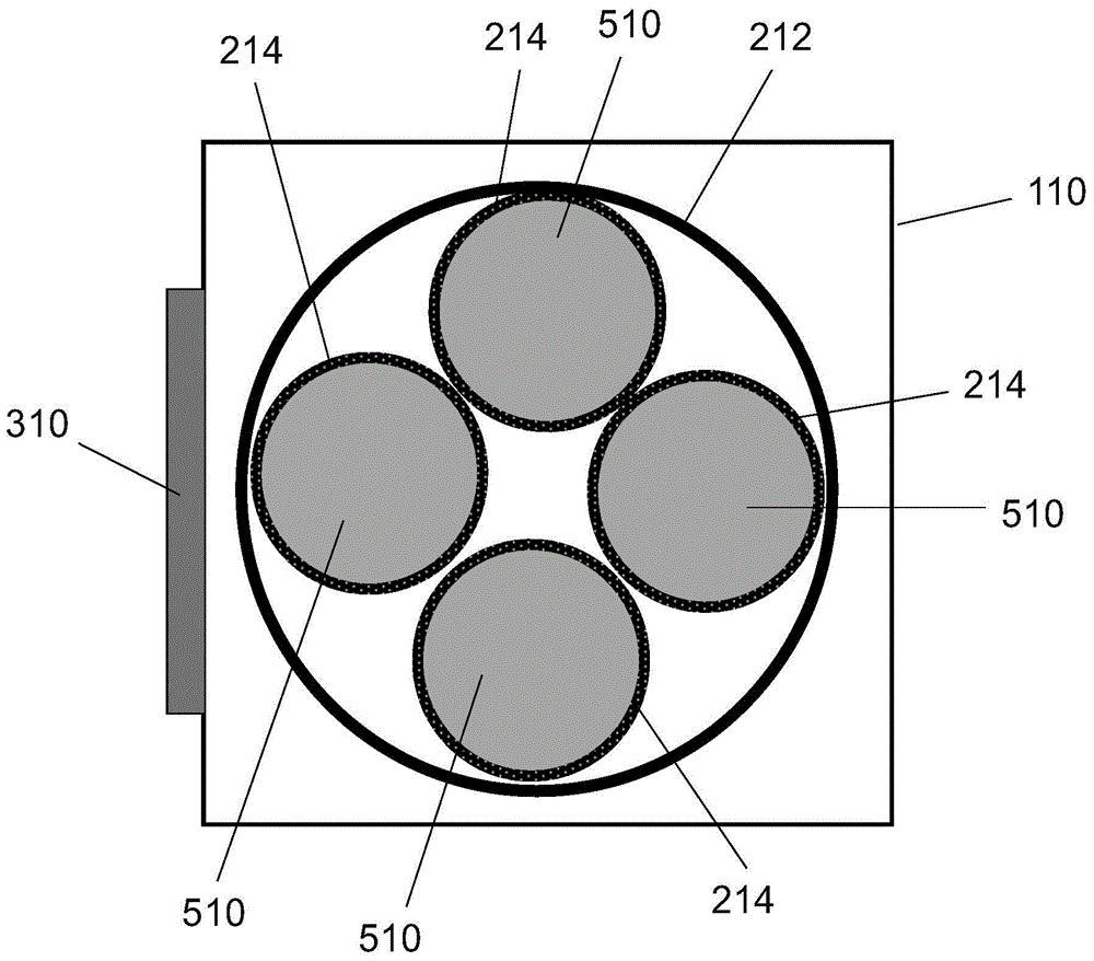
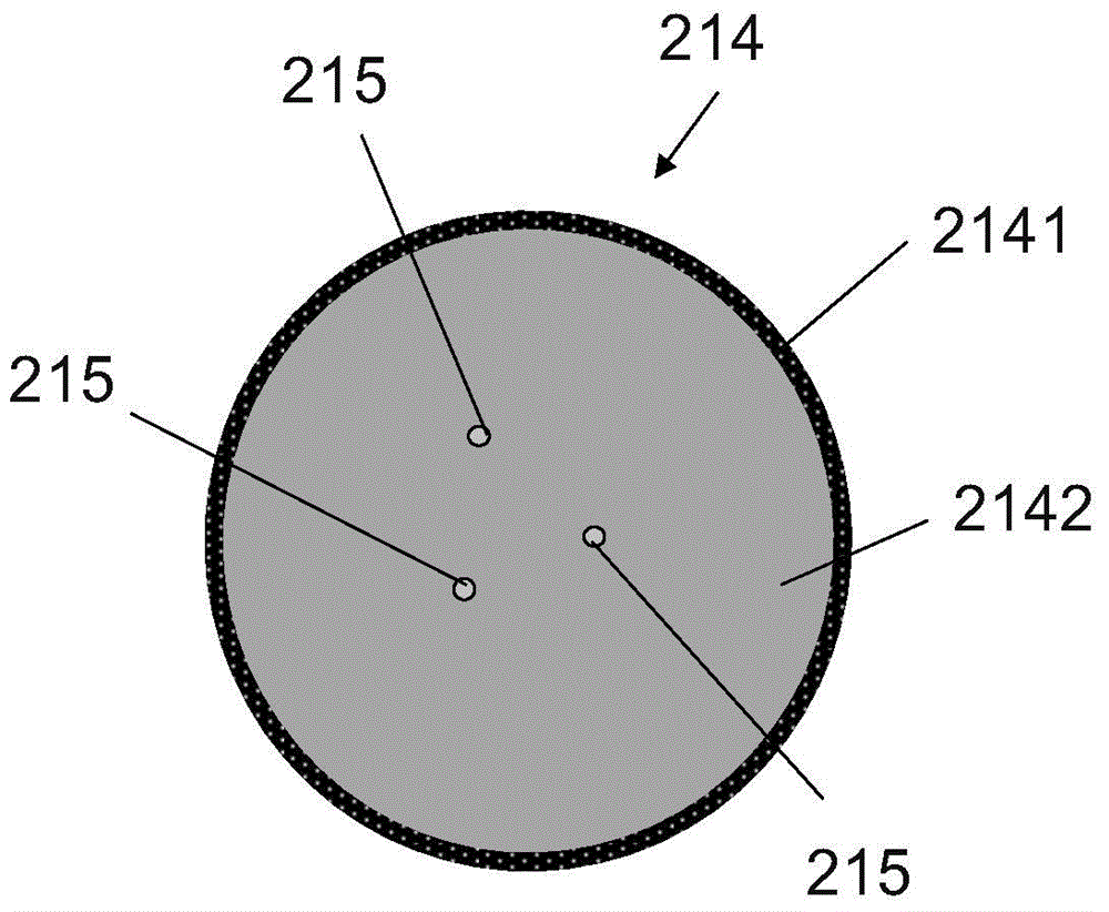
[0028] refer to figure 1 , discloses a schematic cross-sectional structure diagram of the first embodiment of the workpiece processing device of the present invention. Such as figure 1 As shown, the workpiece processing device includes a process chamber 110 and a workpiece carrying mechanism 210 . A "workpiece" as used herein may be a wafer, substrate, substrate, or the like.
[0029] The process chamber 110 has a top wall 111, two pairs of side walls 112 and a bottom wall 113 opposite to the top wall 111. The top wall 111 of the process chamber 110, the two pairs of side walls 112 and the bottom wall 113 form a space to accommodate Workpieces are processed. A side wall 112 of the process chamber 110 is provided with a workpiece inlet ...
PUM
 Abstract
Description
Claims
Application Information