Monitoring device and monitoring method of photoresist surplus, and chip manufacturing device

A monitoring device and photoresist technology are applied in the field of chip manufacturing devices and monitoring devices for the remaining amount of photoresist, which can solve the problem that the remaining amount of photoresist cannot be monitored.

Active Publication Date: 2015-05-27
SEMICON MFG INT (SHANGHAI) CORP
View PDF4 Cites 4 Cited by
  • Summary
  • Abstract
  • Description
  • Claims
  • Application Information

AI Technical Summary

Problems solved by technology

[0006] The purpose of this application is to provide a monitoring device, monitoring method and chip manufacturing device for the remaining amount of photoresist, so as to solve the problem that the remaining amount of photoresist cannot be monitored in the prior art

Method used


Image

  • Monitoring device and monitoring method of photoresist surplus, and chip manufacturing device
  • Monitoring device and monitoring method of photoresist surplus, and chip manufacturing device
  • Monitoring device and monitoring method of photoresist surplus, and chip manufacturing device

Examples


Embodiment Construction

[0033] The embodiments of the application will be described in detail below with reference to the accompanying drawings, but the application can be implemented in many different ways defined and covered by the claims.

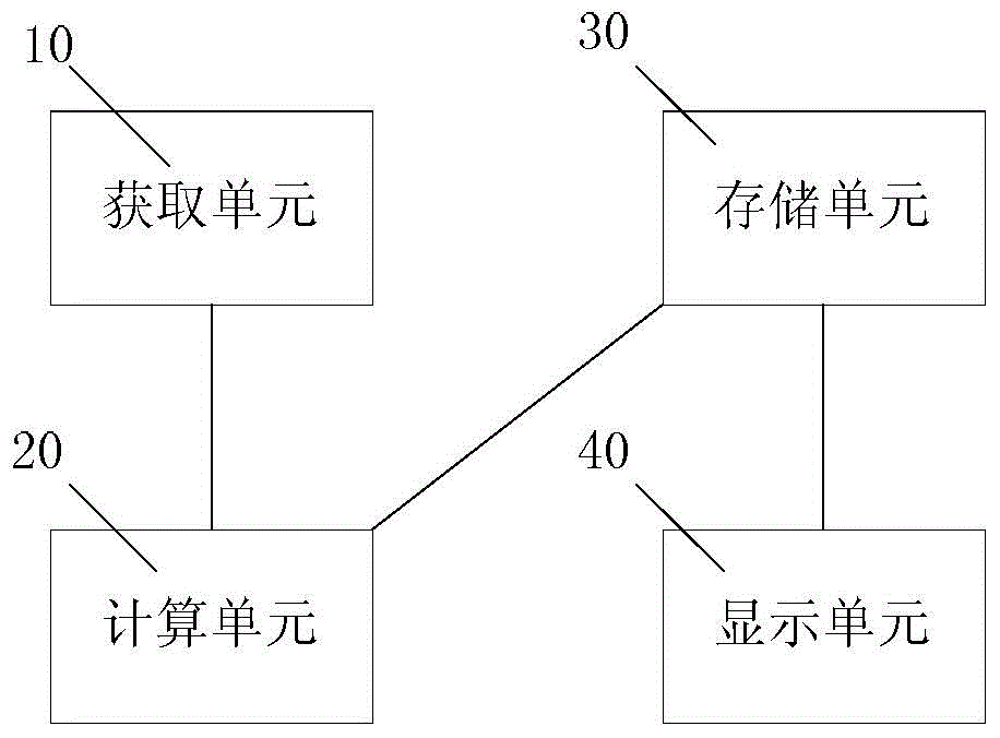
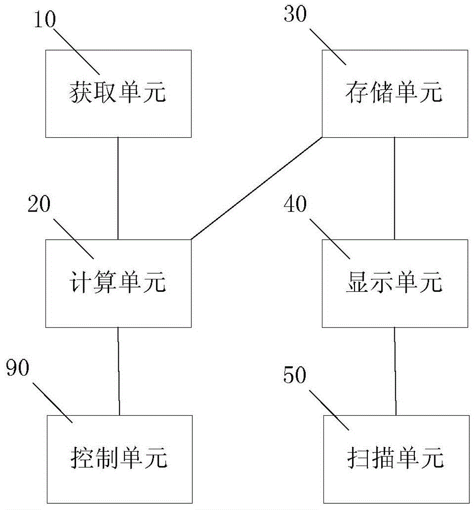
[0034] In order to solve the problem that the remaining amount of photoresist cannot be monitored as pointed out in the background art, a device for monitoring the remaining amount of photoresist is proposed in this application. like figure 1 As shown, the monitoring device includes: an acquisition unit 10, to acquire the shipment quantity of various types of products; a calculation unit 20, connected to the acquisition unit 10, to obtain the quantity according to the shipment quantity of various types of products and the usage of various types of products The unit product photoresist dosage of photoresist and the photoresist initial quantity of every kind of photoresist determine the photoresist residual quantity of every kind of photoresist; Storage unit 30 i...


PUM


Abstract

The invention provides a monitoring device and a monitoring method of photoresist surplus, and a chip manufacturing device. The monitoring device comprises an acquisition unit, a computing unit and a storage unit, wherein the acquisition unit is used for acquiring the shipping quantity of various products; the computing unit is connected with the acquisition unit, and used for determining the photoresist surplus of each photoresist according to the shipping quantity of the various products, the unit photoresist dosage of the different photoresists used by the various products, and the initial quantity of each photoresist; and the storage unit is connected with the computing unit, and used for storing the photoresist surplus of each photoresist and updating the initial quantity of each photoresist. The photoresist surplus of each photoresist can be determined according to the information, so that working personnel can monitor the photoresist surplus in real time, a reliable reference base is provided for the working personnel for reasonable arrangement of a production schedule, use rates of the photoresists are increased, production waste is reduced, and the production efficiency is improved.

Description

technical field [0001] The present application relates to the technical field of semiconductor manufacturing, and more specifically, to a monitoring device, a monitoring method and a chip manufacturing device for remaining amount of photoresist. Background technique [0002] Wafer refers to the silicon wafer used in the production of silicon semiconductor integrated circuits. Because of its circular shape, it is called a wafer; it can be processed into various circuit element structures on the silicon wafer and become a product with specific electrical functions. . [0003] In the process of manufacturing wafers, silicon wafers need to be photolithographically processed. In the prior art, a chip manufacturing device (such as a photolithography machine) is used for photolithography process, and the silicon wafer enters the interior of the chip manufacturing device, and photoresist needs to be coated on the surface of the deposited silicon wafer for photolithography. [0004...

Claims


Application Information

Patent Timeline
Patent Type & Authority Applications(China)
IPC IPC(8): H01L21/66
Inventor 方利黄亮张宛铮
Owner SEMICON MFG INT (SHANGHAI) CORP
Why Eureka
Try Eureka