Manufacturing method of memory

A manufacturing method and memory technology, which is applied in the field of memory manufacturing, can solve problems such as the compression of the landing area of ​​the contact plug, the impact on the formation of the contact plug, and the exposure of metal silicide, and achieve the effect of good element characteristics

Active Publication Date: 2017-05-24
WINBOND ELECTRONICS CORP
View PDF4 Cites 0 Cited by
  • Summary
  • Abstract
  • Description
  • Claims
  • Application Information

AI Technical Summary

Problems solved by technology

If the sidewall of the gate is etched, the metal silicide will be exposed, which will affect the electrical characteristics of the memory
Therefore, in the memory structure with metal silicide formed on the gate and source / drain regions of the peripheral region, the spacer (sidewall) of the gate cannot be etched, which affects the formation of subsequent contact plugs
Therefore, when the size of the memory is further reduced, there will be a problem that the landing area of ​​the contact plug is compressed.

Method used


Image

  • Manufacturing method of memory
  • Manufacturing method of memory
  • Manufacturing method of memory

Examples


Embodiment Construction

[0028] The manufacture and use of the embodiments of the present invention are described below. Embodiments of the invention provide many suitable inventive concepts that may be broadly implemented in a variety of specific contexts. The specific embodiments disclosed are only used to illustrate the making and use of the present invention in specific ways, and are not intended to limit the scope of the present invention.

[0029] It is to be appreciated that the following disclosure of this specification provides many different embodiments, or examples, for implementing the various features of the invention. However, the following disclosures in this specification describe specific examples of each component and its arrangement in order to simplify the description of the invention. Of course, these specific examples are not intended to limit the present invention. For example, if the following disclosure in this specification describes that a first feature is formed on or abo...


PUM

PropertyMeasurementUnit
thicknessaaaaaaaaaa

Abstract

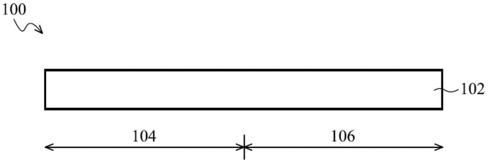
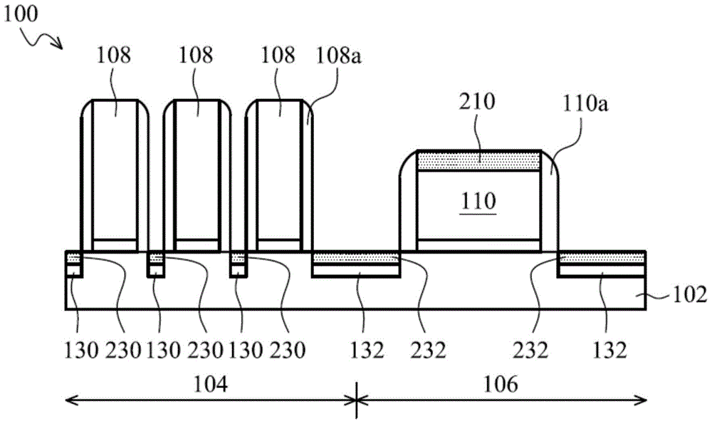
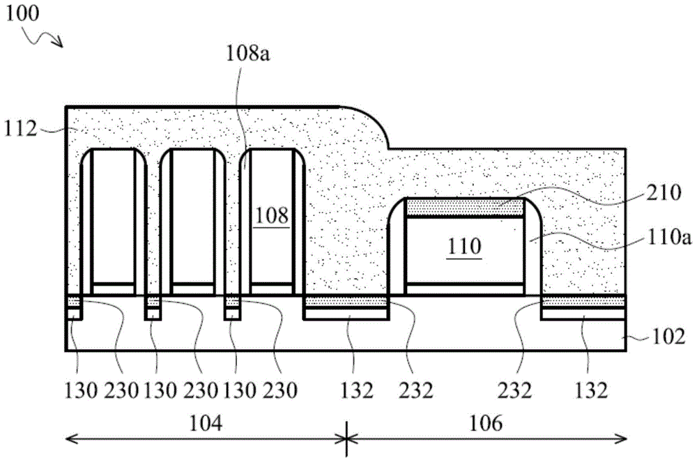
The invention relates to a manufacture method of a storage device. The manufacture method comprises the steps of providing a substrate, wherein the substrate comprises a storage unit area and a peripheral area; forming a plurality of first grid electrodes in the storage unit area and forming at least one second grid electrode in the peripheral area; forming a sacrifice layer on the substrate; forming a first stop layer on the sacrifice layer in the storage unit area; carrying out the etching process by adopting the first stop layer as a mask; sequentially forming a second stop layer on the substrate; depositing a dielectric material on the second stop layer; carrying out the flattening process for the dielectric material by adopting the first stop layer and the second stop layer in the storage unit area as a grinding stop layer; removing the first stop layer and the second stop layer in the storage unit area; removing the sacrifice layer in the storage unit area so as to forming a plurality of first contact openings among the first grid electrodes after the first stop layer and the second stop layer are removed. The stop layers in different thicknesses are formed in the storage unit area and the peripheral area, so that a landing area contacting a plug is not compressed while the size of the storage device is further reduced.

Description

technical field [0001] The invention relates to a manufacturing method of a memory. Background technique [0002] Generally speaking, as the size of the memory gradually shrinks, in order to overcome the increasingly smaller line width and prevent misalignment of the contact plugs, self-aligned contact plugs (self-aligned contacts, SAC) will be used. craft. [0003] In the self-aligned contact plug process, the thickness of the sidewall of the gate affects the size of the contact plug formed between the gates. The memory device includes a memory cell area and a peripheral area. Generally speaking, gates are formed in the memory cell area and the peripheral area at the same time. Afterwards, an etching process is performed on the sidewall of the gate to facilitate subsequent formation of contact plugs. [0004] However, in some memory structures, metal silicides are formed on the gate, source, and drain regions in the peripheral region. If the etching process is performed...

Claims


Application Information

Patent Timeline
Patent Type & Authority Patents(China)
IPC IPC(8): H01L27/115
Inventor 廖修汉蔡耀庭洪文陈彦名
Owner WINBOND ELECTRONICS CORP
Why Eureka
Try Eureka