OLED (Organic Light Emitting Diode) unit, manufacturing method of OLED unit and display panel

A substrate and pixel area technology, which is applied in semiconductor/solid-state device manufacturing, electrical components, semiconductor devices, etc., can solve the problems of pixel area misalignment, display panel color mixing, etc., to reduce the difficulty of alignment, increase the area, and avoid color mixing. Effect

Inactive Publication Date: 2015-06-03
BOE TECH GRP CO LTD
View PDF6 Cites 11 Cited by
  • Summary
  • Abstract
  • Description
  • Claims
  • Application Information

AI Technical Summary

Problems solved by technology

[0005] With the improvement of the resolution of the display panel, more OLED units need to be placed on the display panel of the same size, so that the volume of the OLED unit becomes smaller and smaller. When the anode layer and the electroluminescence unit are aligned It is easy to displace the light-emitting layer and its corresponding pixel area, and the display panel composed of these dislocated OLED units will appear color mixing phenomenon when displaying

Method used


Image

  • OLED (Organic Light Emitting Diode) unit, manufacturing method of OLED unit and display panel
  • OLED (Organic Light Emitting Diode) unit, manufacturing method of OLED unit and display panel
  • OLED (Organic Light Emitting Diode) unit, manufacturing method of OLED unit and display panel

Examples


Embodiment Construction

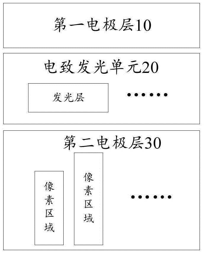
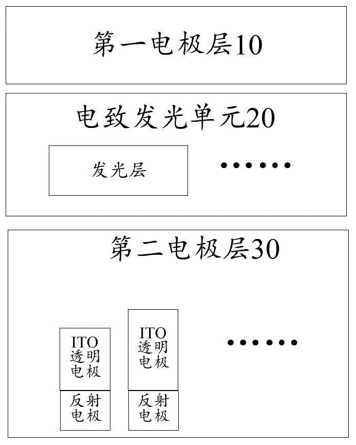
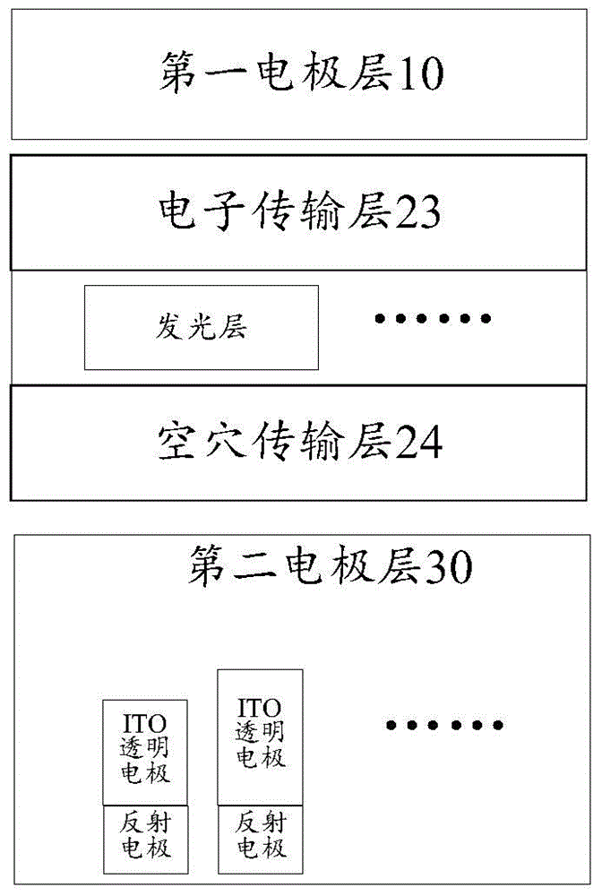
[0038] In order to make the purpose, technical solutions and advantages of the embodiments of the present invention clearer, the technical solutions in the embodiments of the present invention will be clearly and completely described below in conjunction with the drawings in the embodiments of the present invention. Obviously, the described embodiments It is a part of embodiments of the present invention, but not all embodiments. Based on the embodiments of the present invention, all other embodiments obtained by persons of ordinary skill in the art without creative efforts fall within the protection scope of the present invention.

[0039] Unless otherwise defined, the technical terms or scientific terms used herein shall have the usual meanings understood by those skilled in the art to which the present invention belongs. "First", "second" and similar words used in the patent application specification and claims of the present invention do not indicate any order, quantity or...


PUM


Abstract

The invention discloses an OLED (Organic Light Emitting Diode) unit, a manufacturing method of the OLED unit and a display panel and belongs to the technical field of display. The OLED unit comprises a first electrode layer, an electroluminescent unit and a second electrode layer, wherein the electroluminescent unit is located between the first electrode layer and the second electrode layer and comprises at least one luminous layer; each luminous layer corresponds to two pixel areas; the second electrode layer comprises the pixel areas; and each luminous layer is overlapped with the two pixel areas corresponding to a projection area in the second electrode layer. According to the unit, each luminous layer can correspond to the two pixel areas, the quantity of the luminous layers in the OLED unit is reduced, and the area of the luminous layers is increased, so that the alignment difficulty between the luminous layers and the pixel areas is reduced, and a color mixture phenomenon of the display panel is avoided.

Description

technical field [0001] The invention relates to the field of display technology, in particular to an OLED unit, a manufacturing method thereof, and a display panel. Background technique [0002] An OLED (Organic Light-Emitting Diode, Organic Light-Emitting Diode) unit is an organic diode with self-luminous characteristics, which is an important material for manufacturing a display screen. For example, a display panel is an important component of a display screen, and the display panel is composed of a large number of OLED units. [0003] At present, the structure of an OLED unit includes: an anode layer, an electroluminescence unit, and a cathode layer. The electroluminescence unit is located between the anode layer and the cathode layer. The electroluminescence unit includes a plurality of light-emitting layers. A pixel area of ​​the anode layer, the projected area of ​​the light emitting layer on the anode layer overlaps with the corresponding pixel area of ​​the light em...

Claims


Application Information

Patent Timeline
Patent Type & Authority Applications(China)
IPC IPC(8): H01L51/52H01L51/56H01L27/32
CPCH10K59/351H10K50/852H10K50/11H10K59/121H10K50/13H10K50/15H10K50/16H10K50/805H10K71/00H10K59/1201
Inventor 吴长晏闫光万想
Owner BOE TECH GRP CO LTD
Why Eureka
Try Eureka