Shifting register and array substrate grid drive device
A shift register and gate connection technology, applied in static memory, digital memory information, instruments, etc., can solve the problems of reducing stability, changing to low level, and PD point voltage signal attenuation, so as to reduce attenuation, The effect of reducing work loss and improving stability
- Summary
- Abstract
- Description
- Claims
- Application Information
AI Technical Summary
Problems solved by technology
Method used
Image
Examples
Embodiment 1
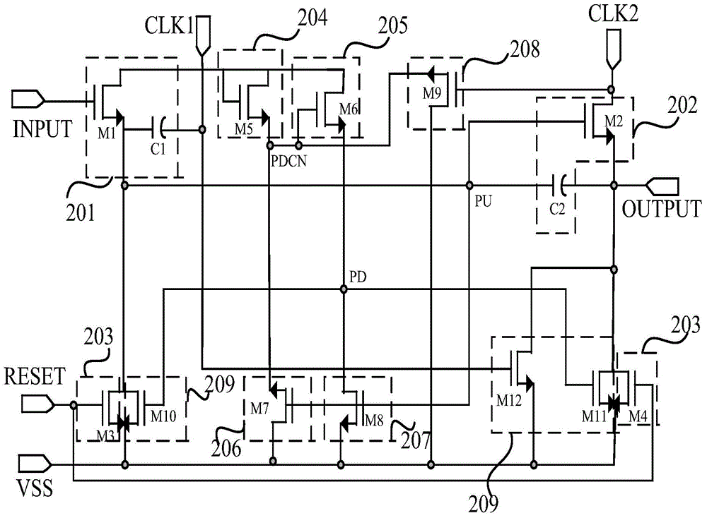
[0051] see figure 2 , a shift register provided by an embodiment of the present invention, wherein the same shift register unit is connected in multiple stages, and the shift register unit includes:
[0052] The input module 201, in response to the input signal INTPUT, is used to provide the first clock signal voltage CLK1 to the pull-up node PU point, wherein the pull-up node is an output node of the input module; including:
[0053] The gate of the first thin film transistor M1 is connected to the input signal terminal, the source is connected to the first clock signal terminal, and the drain is used as the output node of the input module, that is, as the pull-up node PU point;
[0054] The first capacitor C1 is connected between the drain of the first thin film transistor and the first clock signal terminal CLK1;
[0055] The output module 202, in response to the pull-up node PU, is used to provide the second clock signal voltage CLK2 to the output terminal OUTPUT; includ...
Embodiment 2
[0085] see Figure 4 , a cascaded structure diagram of an array substrate gate driving device provided by an embodiment of the present invention, wherein the shift register unit of the cascaded structure takes the shift register provided in Embodiment 1 as an example, wherein,
[0086] If the entire gate drive circuit has a total of N levels of shift register units (GOA units), N is the number of gate lines, and the INPUT of the first level is provided by the vertical turn-on signal (Start Vertical, STV), and the RESET signal of the first level Provided by the OUTPUT of the second stage, the INPUT of the Nth stage is provided by the output of the N-1 stage, and the RESET signal of the Nth stage is provided by the RESET unit. For example, the input signal INTPUT of the nth stage (1
[0087]In summary, in the shift register provi...
PUM
 Abstract
Description
Claims
Application Information


