
Array substrate and its forming method

A technology of array substrates and shift registers, which is applied in digital memory information, instruments, calculations, etc., to achieve the effects of narrow frame design, reduced width, and reduced area

Active Publication Date: 2017-10-03
SHANGHAI AVIC OPTOELECTRONICS +1
View PDF10 Cites 0 Cited by
  • Summary
  • Abstract
  • Description
  • Claims
  • Application Information

AI Technical Summary

Problems solved by technology

It can be seen that the gate drive circuit becomes an obstacle to the narrow frame design of the array substrate, that is, it becomes an obstacle to the narrow frame design of the display panel.

Method used


Image

  • Array substrate and its forming method
  • Array substrate and its forming method
  • Array substrate and its forming method

Examples


Embodiment Construction

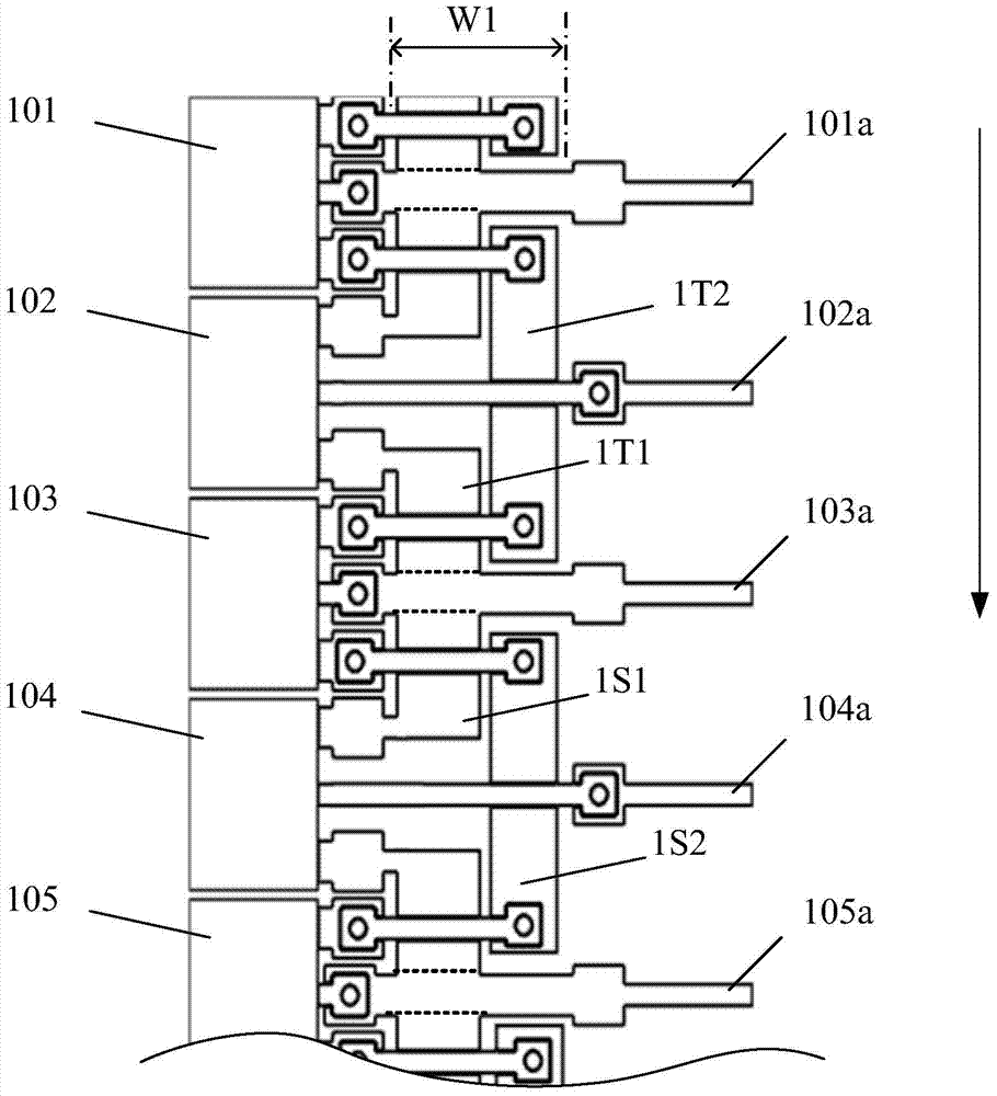
[0026] figure 1 It is a schematic structural diagram of a partial top view of an array substrate, showing a part of the non-display area of ​​the array substrate. The non-display area has a gate drive circuit. The gate drive circuit includes a shift register circuit. The shift register circuit includes two shift register groups, namely a first shift register group and a second shift register group. Both of the shift register groups include a plurality of shift registers. figure 1 The shift register 101 to the shift register 105 are shown as representatives in , and their gate output terminals are respectively the gate output terminal 101a to the gate output terminal 105a. Wherein, an odd number of shift registers belongs to the first shift register group, that is, the shown shift register 101 , shift register 103 and shift register 105 all belong to the first shift register group. An even number of shift registers belongs to the second shift register group, that is, both t...


PUM


Abstract

An array substrate and a method of forming the same. Wherein, the array substrate includes: a gate drive circuit located in a non-display area, the gate drive circuit includes M shift register circuits, each of the shift register circuits has two shift register groups, each The shift register group has N shift registers, where M is a positive even number and N is a positive integer greater than 2; in each of the shift register groups, the gate output end of the nth shift register has a signal Routing: In the direction perpendicular to the non-display area, at least one signal routing of the shift register group is located above the signal routing of another of the shift register groups. Display panels using this array substrate can achieve narrow bezel designs.

Description

technical field [0001] The present invention relates to the field of display technology, in particular to an array substrate and a forming method thereof. Background technique [0002] Liquid crystal display (liquid crystal display, LCD) or organic light-emitting diode (Organic Light-Emitting Diode, OLED) display has the advantages of low radiation, small size and low power consumption, etc., and is widely used in notebook computers, personal digital assistants (Personal Digital Assistants). Assistant, PDA), flat-screen TVs and mobile phones and other information products. [0003] Taking a liquid crystal display as an example, an external driver chip is used to drive chips on a panel to display images. However, in order to reduce the number of components and reduce the manufacturing cost, in recent years, the driving circuit structure has been gradually developed to be directly fabricated on the display panel. For example, a technology of integrating a gate driver into an...

Claims


Application Information

Patent Timeline
Patent Type & Authority Patents(China)
IPC IPC(8): G09G3/36
CPCG11C19/287G06F3/0412G06F3/044G06F3/04164G06F3/04184G06F2203/04103G06F3/047
Inventor 金慧俊
Owner SHANGHAI AVIC OPTOELECTRONICS
Features
  • Generate Ideas
  • Intellectual Property
  • Life Sciences
  • Materials
  • Tech Scout
  • Unparalleled Data Quality
  • Higher Quality Content
  • 60% Fewer Hallucinations
Learn More