Array substrate and display device

A technology of array substrate and display area, applied in nonlinear optics, instruments, optics, etc., can solve problems such as display mura and reduction of SourceBorder width.

Inactive Publication Date: 2020-10-20
TCL CHINA STAR OPTOELECTRONICS TECH CO LTD
View PDF6 Cites 1 Cited by
  • Summary
  • Abstract
  • Description
  • Claims
  • Application Information

AI Technical Summary

Problems solved by technology

This method of using the width of 2 sub-pixels for the first-level GOA circuit layout reduces the width of the Source Border; but the

Method used


Image

  • Array substrate and display device
  • Array substrate and display device
  • Array substrate and display device

Examples


Embodiment Construction

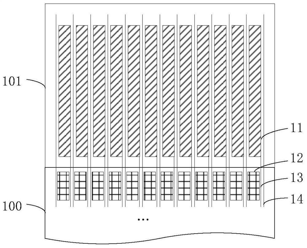
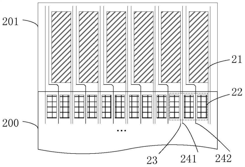
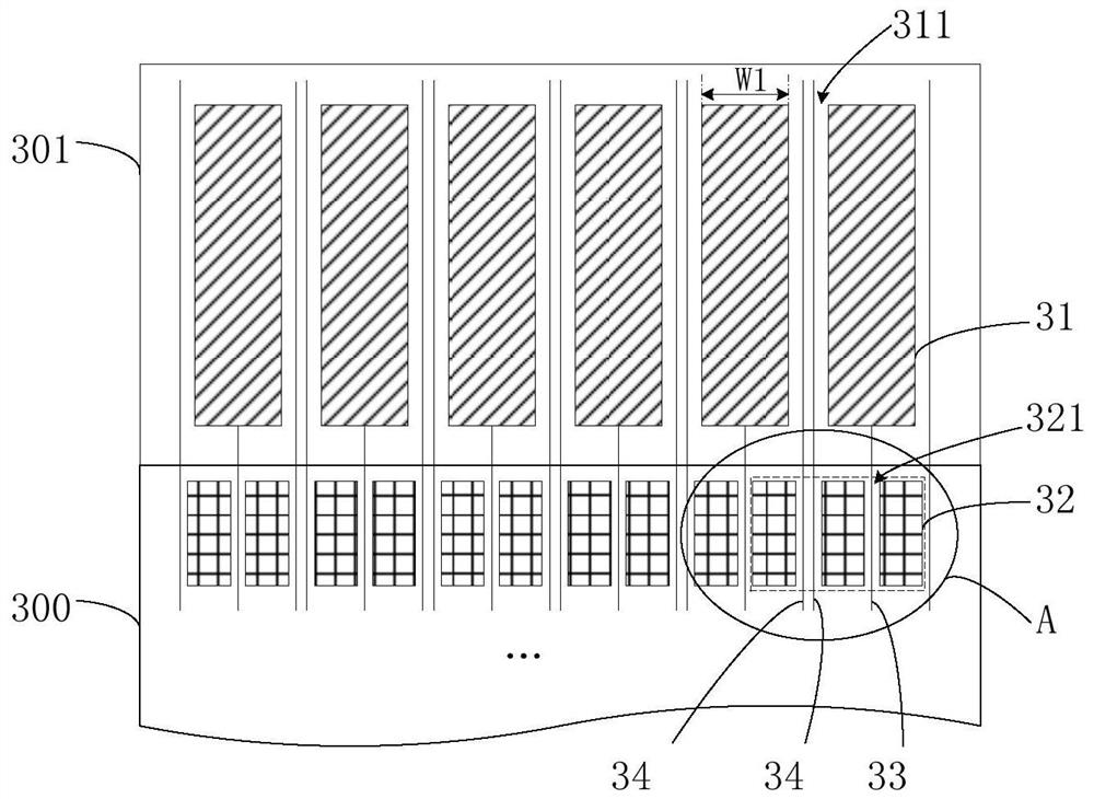
[0019] Embodiments of the present application are described in detail below, examples of which are shown in the drawings, wherein the same or similar reference numerals denote the same or similar components or components having the same or similar functions throughout. The terms "first", "second", "third", etc. (if any) in the description and claims of this application and the drawings are used to distinguish similar objects and not necessarily to describe a specific order or sequence . It should be understood that the items so described are interchangeable under appropriate circumstances. In the description of the present application, "plurality" means two or more, unless otherwise specifically defined. Furthermore, the terms "comprising" and "having", as well as any variations thereof, are intended to cover a non-exclusive inclusion. The directional terms mentioned in this application, such as: up, down, left, right, front, back, inside, outside, side, etc., are only direc...


PUM


Abstract

The invention discloses an array substrate and a display device. According to the invention, a flip pixel architecture for wiring in a DD + G mode is adopted, and a GOA circuit is arranged on a sourcedriving side; since the two data lines are adjacent and enter the AA area in parallel, the gate fan-out lead and the two data lines enter the AA area in a parallel but non-adjacent manner, and signalcoupling between the gate fan-out lead and the data lines is prevented. By using the widths of two pixel units to carry out the first-stage GOA circuit layout, the realization of a narrow frame is facilitated.

Description

technical field [0001] The present application relates to the field of display technology, in particular to an array substrate and a display device. Background technique [0002] Liquid Crystal Display (LCD for short) has been widely used in computer screens, TV screens, mobile digital phones and other fields due to its advantages of light and thin body, low energy consumption, low working voltage and no radiation. . [0003] With the continuous development of liquid crystal display technology, people have higher and higher requirements for display devices. In response to market demands, large size, high resolution, and Ultra Narrow Border (UNB for short) have become a market trend. The ultra-narrow bezel is to further expand the area of ​​the active display area (Active Area, referred to as AA) by further compressing the width of the bezel area. The requirement of ultra-narrow bezels poses higher challenges to the design and manufacture of LCDs. [0004] In recent years...

Claims


Application Information

Patent Timeline
IPC IPC(8): G02F1/1345G02F1/1362
CPCG02F1/13454G02F1/1362G02F1/136286G09G3/20G09G3/3677G09G2300/0426G09G2300/0408G09G3/3688G09G2320/0233
Inventor 王添鸿钟云肖金一坤
Owner TCL CHINA STAR OPTOELECTRONICS TECH CO LTD
Why Eureka
Try Eureka