A wafer alignment mark
A technology for aligning marks and wafers, applied in electrical components, electrical solid-state devices, circuits, etc., can solve the problems of affecting the bonding accuracy of wafers, occupying the effective area of the chip, reducing the effective area of the chip, etc. area effect
- Summary
- Abstract
- Description
- Claims
- Application Information
AI Technical Summary
Problems solved by technology
Method used
Image
Examples
Embodiment Construction
[0017] The present invention will be further described below in conjunction with the accompanying drawings and specific embodiments, but not as a limitation of the present invention.
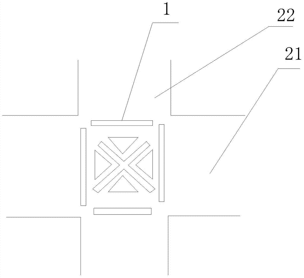
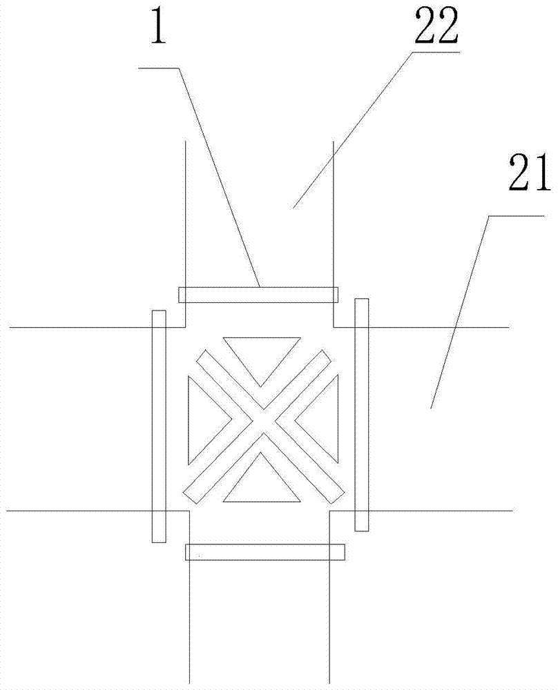
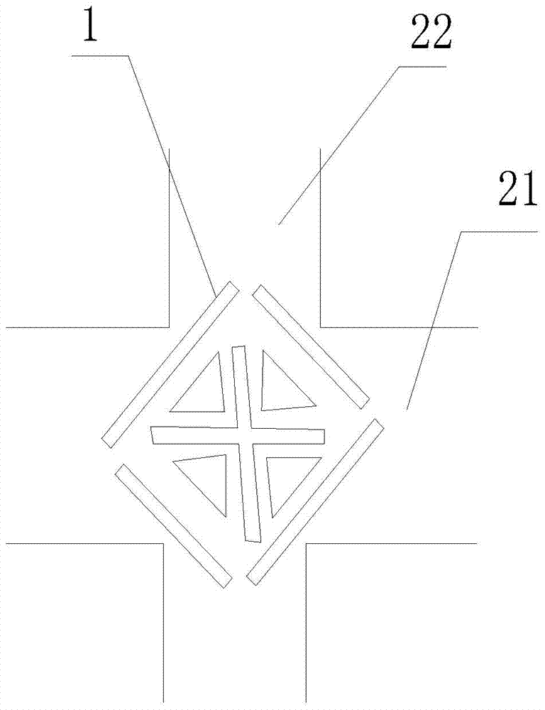
[0018] The invention discloses a wafer alignment mark. The alignment mark can be applied in the bonding process of wafers. The wafer is provided with cutting lines intersecting each other, and a tip pattern is provided on the crossing area of the cutting lines. alignment marks, and the tip pattern extends into non-intersecting areas of the dicing lanes.
[0019] In a preferred embodiment of the present invention, the above-mentioned cutting lines may include horizontal cutting lines and vertical cutting lines perpendicular to each other.
[0020] On this basis, further, the angle formed between the alignment mark and the horizontal cutting line is not 0°, preferably, the value range of the angle between the alignment mark and the horizontal cutting line is 30°-60°( For example 30°, 45°, 50° o...
PUM
 Abstract
Description
Claims
Application Information


