Array substrate, manufacture method for array substrate and display device

A technology of array substrates and substrates, which is applied in semiconductor/solid-state device manufacturing, semiconductor/solid-state device testing/measurement, semiconductor devices, etc., can solve problems such as accumulating charges and damaging working circuits, and achieve the effect of reducing the antenna effect

Active Publication Date: 2015-06-10
BOE TECH GRP CO LTD +1
View PDF4 Cites 10 Cited by
  • Summary
  • Abstract
  • Description
  • Claims
  • Application Information

AI Technical Summary

Problems solved by technology

[0003] In order to solve the problem in the related art that the slender test lines tend to accumulate more charges due to the antenna effect, and these charges may damage the working circuit, the present invention provides an array substrate, a manufacturing method of the array substrate and a display device

Method used


Image

  • Array substrate, manufacture method for array substrate and display device
  • Array substrate, manufacture method for array substrate and display device
  • Array substrate, manufacture method for array substrate and display device

Examples


Embodiment Construction

[0058] Reference will now be made in detail to the exemplary embodiments, examples of which are illustrated in the accompanying drawings. When the following description refers to the accompanying drawings, the same numerals in different drawings refer to the same or similar elements unless otherwise indicated. The implementations described in the following exemplary examples do not represent all implementations consistent with the present invention. Rather, they are merely examples of apparatuses and methods consistent with aspects of the invention as recited in the appended claims.

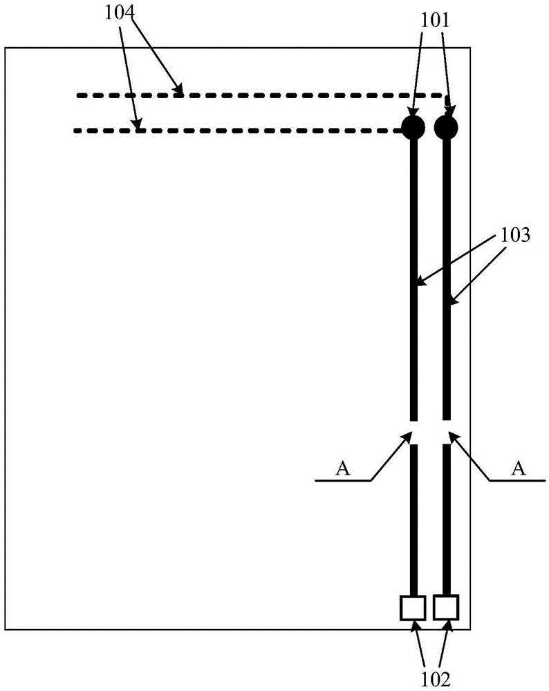
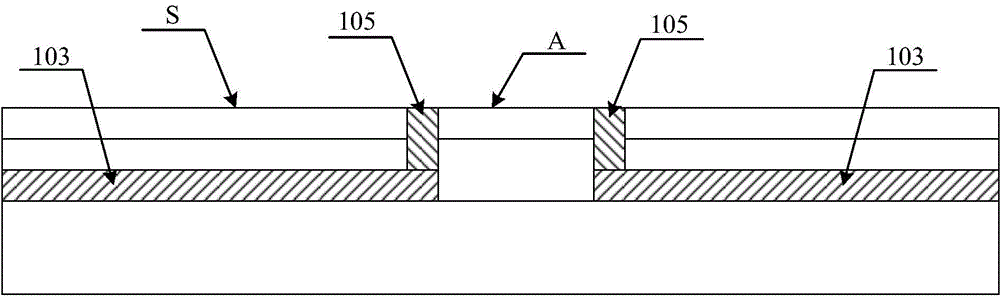
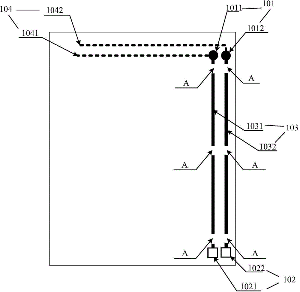
[0059] After research, the inventor found that an array substrate is provided with a test circuit, and the test circuit is respectively connected to the working circuit interface located at one end of the array substrate in the length direction (the working circuit interface is electrically connected to the working circuit) and the The test interface at the other end in the length direction dire...


PUM


Abstract

The invention discloses an array substrate, a manufacture method for an array substrate and a display device and relates to the display technical field. The array substrate comprises a test circuit connected with a work circuit interface and a test interface; the test circuit comprises at least one cut-off point, two ends of each cut-off point on the test circuit are respectively provided with a conductive contact running through the upper surface of the array substrate; while performing the test to the work circuit, the conductive contacts at two ends of all cut-off points are switched on for having breakover for the test circuit. At least one cut-off point is formed on the test circuit during the forming process of the test circuit, and the sub test circuit cut from the cut-off point is not long, so that the antenna effect caused by longer test circuit is reduced, and the problem that the work circuit is damaged by the charge collected by the slender test circuit for the antenna effect of the related technology can be solved; the work circuit is not damaged by the test circuit due to the antenna effect.

Description

technical field [0001] The present invention relates to the field of display technology, in particular to an array substrate, a method for manufacturing the array substrate, and a display device. Background technique [0002] The array substrate is an important part of the display device, and both the display area and the surrounding area of ​​the array substrate are provided with working circuits. Due to the complex structure of some array substrates, such as low temperature polysilicon (English: Low Temperature Poly-Silicon; LTPS for short) array substrates, it is necessary to perform relevant tests on the working circuits on the LTPS array substrates in the production stage. Contents of the invention [0003] In order to solve the problem in the related art that the long and thin test lines tend to accumulate more charges due to the antenna effect, and these charges may damage the working circuit, the present invention provides an array substrate, a manufacturing method...

Claims


Application Information

Patent Timeline
Patent Type & Authority Applications(China)
IPC IPC(8): H01L27/12H01L21/77H01L21/66
CPCH01L22/32H01L22/14H01L27/1244H01L27/1259
Inventor 樊浩原辛燕霞杨玉清
Owner BOE TECH GRP CO LTD
Why Eureka
Try Eureka