Thin film transistor and manufacturing method thereof as well as display device

A technology of thin film transistors and manufacturing methods, which is applied in the direction of transistors, semiconductor/solid-state device manufacturing, semiconductor devices, etc., can solve the problems of increased number of masks, complex processes, and increased costs, so as to reduce the number of patterning processes and reduce manufacturing costs , The effect of saving etching time

Active Publication Date: 2015-06-17
BOE TECH GRP CO LTD
View PDF3 Cites 16 Cited by
  • Summary
  • Abstract
  • Description
  • Claims
  • Application Information

AI Technical Summary

Problems solved by technology

Taking metal oxide TFT as an example, in theory, the manufacturing process of compound semiconductor TFT should be the same as that of amorphous silicon TFT, but in the existing technology, both dry etching and wet etching are vulnerable to chemical stability. The compound semiconductor active layer will cause damage and ultimately affect device performance, that is, the BCE process will damage the compound semiconductor active layer while forming the source and drain electrodes. Therefore, the current BCE process cannot be directly used to prepare compound semiconductor thin film transistors. Increase the preparation process of the etch stop layer used to protect the compound semiconductor active layer, but after adding the etch stop layer, the number of masks required for the preparation process will increase, the process will become complicated, and the cost will increase accordingly

Method used


Image

  • Thin film transistor and manufacturing method thereof as well as display device
  • Thin film transistor and manufacturing method thereof as well as display device
  • Thin film transistor and manufacturing method thereof as well as display device

Examples


Embodiment

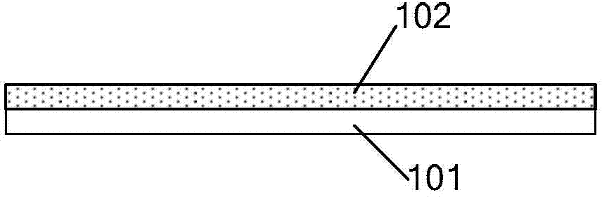
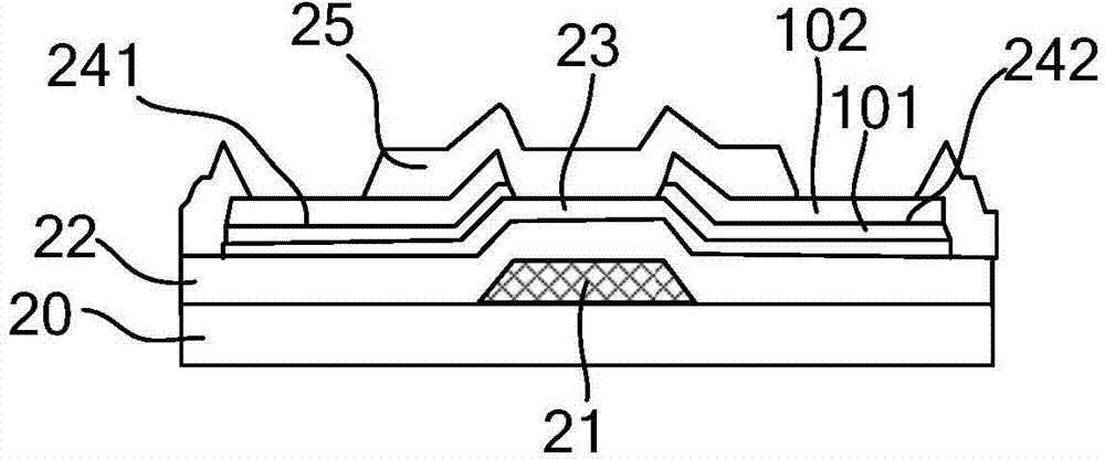
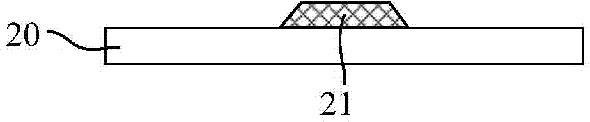
[0040] An embodiment of the present invention provides a thin film transistor, the thin film transistor includes: a gate, an active layer, a source and a drain, the source and the drain are formed of at least two materials, the source and the drain The forming material can undergo cell reaction in the corresponding etching solution to be etched, and the etching solution does not corrode the active layer.

[0041] Aiming at the problem that the active layer of the existing TFT is easily corroded by the etchant used in the source and drain formation process, this embodiment adopts a new solution idea: the material of the source and drain in the thin film transistor is selected to be A material that undergoes a battery reaction in an electrolyte, and at the same time, the electrolyte corresponding to the battery reaction is used as an etching solution in the formation process of the source and drain electrodes, and the electrolyte is used as an etching solution for the thin film t...


PUM


Abstract

The invention discloses a thin film transistor and a manufacturing method thereof as well as a display device, relates to the display field and can solve the problem that an active layer is easy to corrode on a source electrode and a drain electrode in an etching process, so that a thin film transistor device can be prepared with a back channel etching process, the manufacturing process time of the thin film transistor is reduced, and the manufacturing cost is saved. The thin film transistor comprises a grid electrode, an active layer, a source electrode and drain electrode, wherein the source electrode and the drain electrode are made of at least two kinds of materials, cell reaction can occur to the materials of the source electrode and the drain electrode in an etching liquid so that the source electrode and the drain electrode are corroded, and the etching liquid doesn't corrode the active layer.

Description

technical field [0001] The invention relates to the display field, in particular to a thin film transistor, a manufacturing method thereof, and a display device. Background technique [0002] TFT (Thin Film Transistor), a compound semiconductor represented by metal oxide, has the advantages of high mobility, simple manufacturing process, good large-area uniformity, and low manufacturing cost. It is considered to be the driving active material. Matrix Organic Light Emitting Diodes (Active Matrix Organic Light Emitting Diode, AMOLED) show the most promising devices. Therefore, in recent years, the compound semiconductor TFT has attracted the attention of the industry, and has been gradually applied to the AMOLED display panel. [0003] In the manufacturing technology of TFT, the back channel etching (Back Channel Etch, BCE) process is a common process of amorphous silicon TFT, only four photolithography can be used to form TFT: the first photolithography process forms the gat...

Claims


Application Information

Patent Timeline
Patent Type & Authority Applications(China)
IPC IPC(8): H01L29/786H01L21/336H01L29/43
CPCH01L29/45H01L21/28575H01L21/32134H01L21/443H01L21/47635H01L29/20H01L29/2003H01L29/22H01L29/24H01L29/42356H01L29/66522H01L29/66742H01L29/66969H01L29/786H01L29/78681H01L29/7869H01L29/41733
Inventor 王龙彦李永谦曹昆李全虎尹静文张保侠盖翠丽吴仲远王刚
Owner BOE TECH GRP CO LTD
Why Eureka
Try Eureka