Method of preparing a sample for transmission electron microscopy

a transmission electron microscopy and sample technology, applied in the direction of material analysis using wave/particle radiation, semiconductor device details, instruments, etc., can solve the problems of affecting the etching speed of the ion doped regions, the time-consuming sims method, and the damage to the semiconductor devi

Active Publication Date: 2010-01-19
SEMICON MFG INT (SHANGHAI) CORP
View PDF4 Cites 8 Cited by
  • Summary
  • Abstract
  • Description
  • Claims
  • Application Information

AI Technical Summary

Benefits of technology

[0010]An object of the present invention is to provides a method for preparing a TEM sample so as to avoid the problem that it is difficult to distinguish the lightly doped drain, source / drain regions from the silicon substrate and to clearly observe the pattern and defects in the lightly doped drain, source / drain regions, since the lightly doped drain, source / drain regions are in the same thickness as the silicon substrate.
[0016]Because an etching process by acid is added during preparing the TEM sample by FIB, the invention has following advantages over the existing method. Since the lightly doped drain, source / drain regions are ion doped regions, the acid solution will react with the ions in the lightly doped drain, source / drain regions. Since the silicon substrate is a non-doped region, the acid solution will not react with the silicon substrate. Therefore, the etching speed of the ion doped regions by the acid solution is faster than that of the non-doped region. As a result, the lightly doped drain, source / drain regions will be thinner than the silicon substrate after the etching process with acid. When this sample is observed in TEM, it is easy to distinguish the lightly doped drain, source / drain regions from the silicon substrate and to clearly observe the pattern and defects in the lightly doped drain, source / drain regions. Moreover, it is easy to distinguish the boro-phospho-silicate-glass (BPSG) from the non-doped silicon dioxide in the failure regions.

Problems solved by technology

However, implanting a large amount of impurities into the small region by the ion implantation method will cause defects, resulting in a leakage current in the PN junction and then damaging the semiconductor device.
However, the SIMS method usually is time-consuming due to its low detection speed and therefore is not suitable for analyzing a small region.
In addition, the SIMS method can only be used to detect defects in wafers other than semiconductor devices.
Thus the detection result cannot faithfully represent defects in the final products.
Since the lightly doped drain, source / drain regions in the TEM sample prepared by FIB according to existing methods are in the same thickness as the silicon substrate, it is difficult to distinguish the lightly doped drain, source / drain regions from the silicon substrate and to clearly observe the pattern and defects in the lightly doped drain, source / drain regions.

Method used


Image

  • Method of preparing a sample for transmission electron microscopy
  • Method of preparing a sample for transmission electron microscopy
  • Method of preparing a sample for transmission electron microscopy

Examples


first embodiment

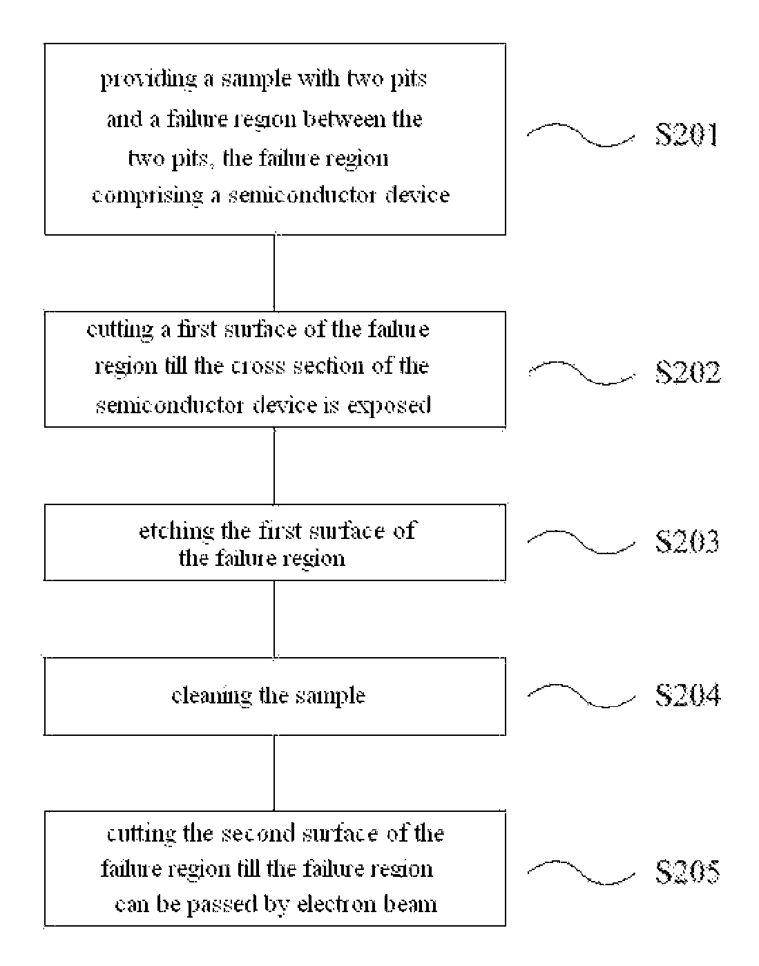
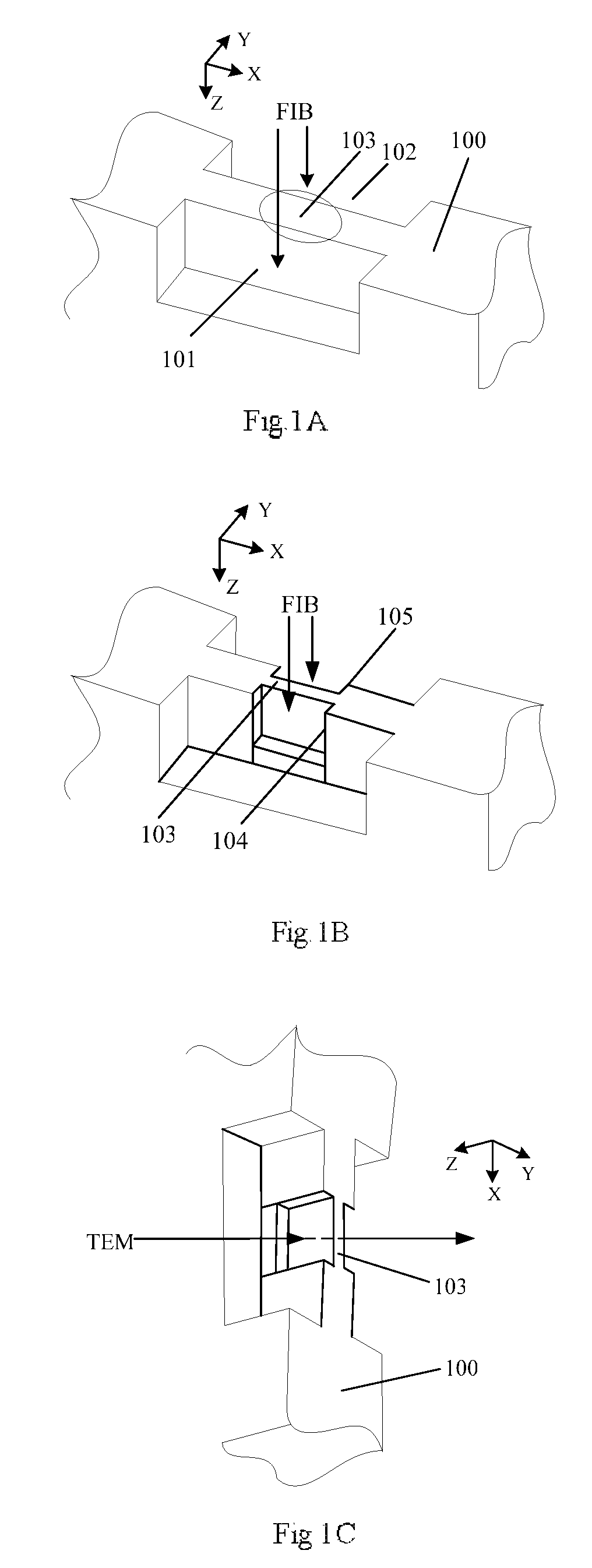
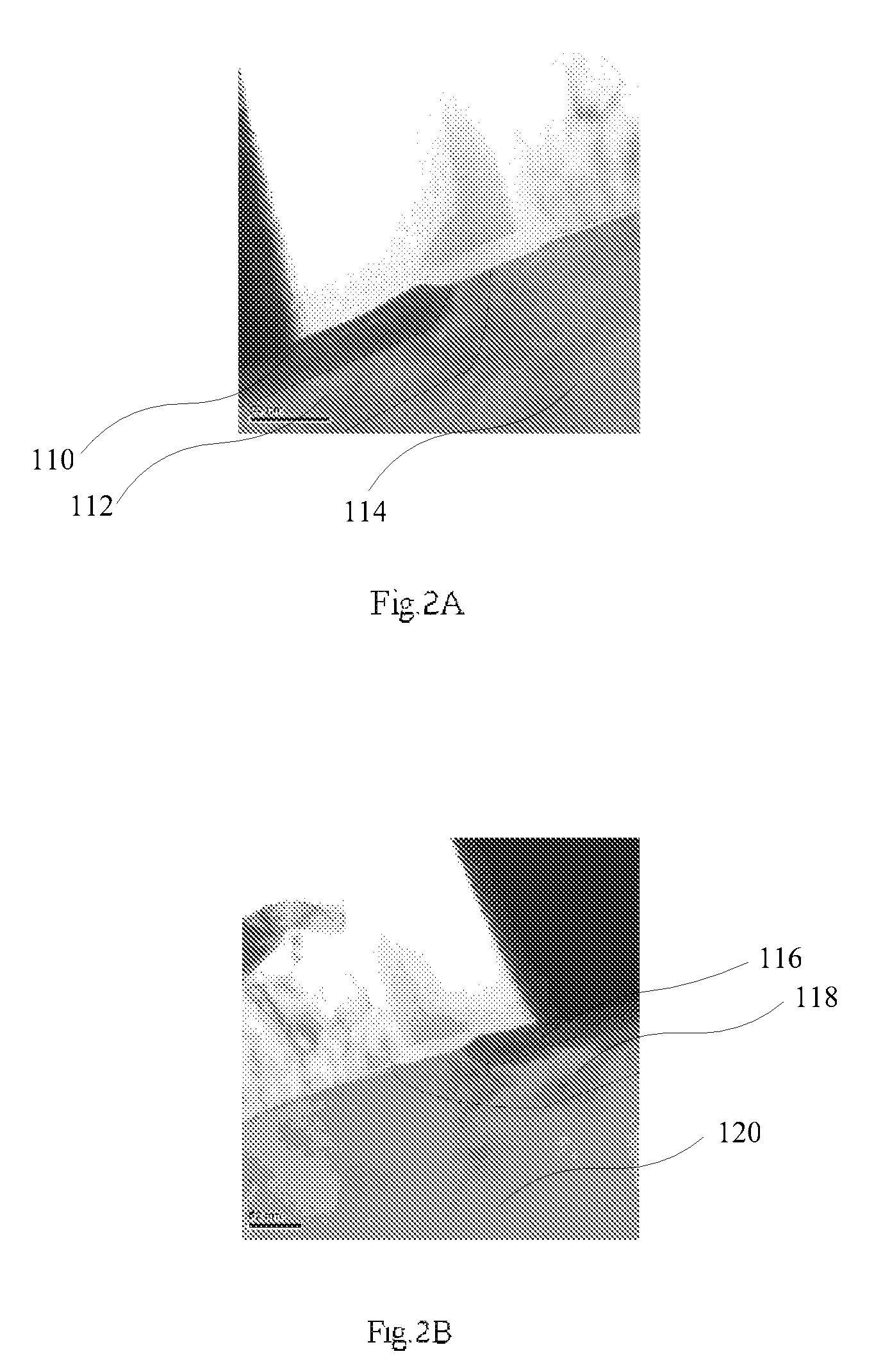
[0024]FIGS. 4A-4D are schematic diagrams of the procedure for preparing TEM samples according to the present invention. In the invention, as shown in FIG. 4A, the failure region 201 is first positioned on the sample 200 using an electrical positioning method, i.e., using an emission microscope (EMMI) or an optical beam induced resistance change (OBIRCH) tool. The sample 200 is placed into the FIB apparatus, and positions and dimensions of the pits are defined by a software in the FIB apparatus. The surface of sample 200 is bombarded by FIB with a current of 500 pA-7000 pA to form the pits 202 and 203 having a larger area than the failure region 201 at both sides of the failure region 201, so that the cross section of the failure region 201 can be observed during the subsequent process for milling the failure region 201, and the failure region 201 can be taken out from the sample 200 easily. The pits 202 and 203 are 10 μm-20 μm in length, 5 μm-10 μm in width, and 2 μm-5 μm in depth. ...

second embodiment

[0035]Next, the method for preparing TEM samples according to the invention is described referring to FIG. 4A to 4D. As shown in FIG. 4A, firstly, the failure region 201 is positioned on the sample 200 by an electrical positioning method, i.e., by means of EMMI or OBIRCH tool; next, the sample 200 is placed into the FIB apparatus, and the positions and dimensions of the pits are defined by a software in the FIB apparatus; next, the surface of the sample 200 is bombarded by FIB with a current of 5000 pA-7000 pA to form pits 202 and 203 having a larger area than the failure region 201 at both sides of the failure region 201, so that the cross section of the failure region 201 can be observed during the subsequent process for milling the failure region 201 and the failure region 201 can be taken out from the sample 200 easily; the pits 202 and 203 are 15 μm in length, 8 μm in width, and 6 μm in depth; the failure region 201 is 1μm.

[0036]As shown in FIG. 4B, the current for FIB is regul...


PUM

PropertyMeasurementUnit
currentaaaaaaaaaa
length×width×depthaaaaaaaaaa
currentaaaaaaaaaa

Abstract

A method for preparing TEM sample, comprising the following steps: providing a sample with two pits and a failure region between the two pits, the failure region comprising a semiconductor device; milling the first surface of the failure region, till the cross section of the semiconductor device is exposed; etching the first surface of the failure region; cleaning the sample; milling the second surface of the failure region, till the failure region can be passed by electron beam. A sample can be prepared for a high resolution TEM through above steps. When the sample is observed, it is easy to distinguish the lightly doped drain, source / drain regions from the silicon substrate and observe the pattern and defects in the lightly doped drain, source / drain regions clearly; in addition, it is easy to distinguish the BPSG from the non-doped silicon dioxide in the failure region.

Description

[0001]This application claims the priority of Chinese Patent Application 200610116910.1, filed Sep. 30, 2006, the entire disclosure of which is incorporated herein by reference.FIELD OF THE INVENTION[0002]The invention relates to a method of preparing a sample for transmission electron microscopy (TEM).BACKGROUND OF THE INVENTION[0003]With the development of Very Large Scale Integration (VLSI), lightly doped drain (LDD) and source / drain regions are employed in deep submicron systems. In order to make the source / drain expansion region shallower so as to control the short channel effect, a large amount of impurities are often used as dopant in an area near the channel of the source / drain PN junction to control the depth of the LDD region and the source / drain expansion region. However, implanting a large amount of impurities into the small region by the ion implantation method will cause defects, resulting in a leakage current in the PN junction and then damaging the semiconductor devi...

Claims


Application Information

Patent Timeline
Patent Type & Authority Patents(United States)
IPC IPC(8): G01N23/00G21K7/00
CPCG01N1/32
Inventor HU, JIANQIANGRUI, ZHIXIANZHAO, YANLIWANG, YANJUNLI, MINGPAN, MIN
Owner SEMICON MFG INT (SHANGHAI) CORP
Why Eureka
Try Eureka