

Antireflection film composition and patterning process using the same
- Summary
- Abstract
- Description
- Claims
- Application Information
AI Technical Summary
Benefits of technology
Problems solved by technology
Method used
Image


Examples
synthesis example 1
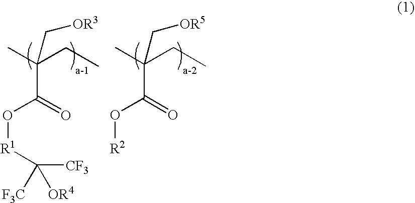
[0166]In a 100 mL flask, 9.3 g of monomer 1, 5.7 g of 2,3-epoxypropyl methacrylate ester, 3.1 g of styrene, and 20 g of tetrahydrofuran as a solvent were added. This reaction vessel was cooled to −70° C. under a nitrogen atmosphere, and deaeration under reduced pressure and nitrogen flowing were repeated three times. 0.1 g of AIBN as a polymerization initiator was added as a polymerization initiator after elevating to a room temperature, and then it was elevated to 60° C. and reacted for 15 hours. This reaction solution was poured in 100 mL of isopropyl alcohol to precipitate. A obtained white solid was filtrated, and then dried at 60° C. under reduced pressure to yield a white polymer.
[0167]The obtained polymer was analyzed by 13C, 1H-NMR and GPC, and the following results were obtained.
[0168]Polymerization ratio: monomer 1:2,3-epoxypropyl methacrylate ester:styrene=0.3:0.4:0.3
[0169]Molecular weight (Mw)=9,000
[0170]Dispersion degree (Mw / Mn)=1.60
This polymer was designated as polyme...
synthesis example 2
[0171]In the 100 mL flask, 8.5 g of monomer 2, 5.7 g of 2,3-epoxypropyl methacrylate ester, 3.1 g of styrene, and 20 g of tetrahydrofuran as a solvent were added. This reaction vessel was cooled to −70° C. under a nitrogen atmosphere, and deaeration under reduced pressure and nitrogen flowing were repeated three times. 0.1 g of AIBN as a polymerization initiator was added as a polymerization initiator after elevating to a room temperature, and then it was elevated to 60° C. and reacted for 15 hours. This reaction solution was poured in 100 mL of isopropyl alcohol to precipitate. A obtained white solid was filtrated, and then dried at 60° C. under reduced pressure to yield a white polymer.
[0172]The obtained polymer was analyzed by 13C, 1H-NMR and GPC, and the following results were obtained.
[0173]Polymerization ratio: monomer 2:2,3-epoxypropyl methacrylate ester:styrene=0.3:0.4:0.3
[0174]Molecular weight (Mw)=9,300
[0175]Dispersion degree (Mw / Mn)=1.82
This polymer was designated as poly...
synthesis example 3
[0176]In the 100 mL flask, 4.7 g of monomer 1, 2.8 g of monomer 4, 5.2 g of 2-hydroxyethyl methacrylate ester, 3.1 g of styrene, and 20 g of tetrahydrofuran as a solvent were added. This reaction vessel was cooled to −70° C. under a nitrogen atmosphere, and deaeration under reduced pressure and nitrogen flowing were repeated three times. 0.1 g of AIBN as a polymerization initiator was added as a polymerization initiator after elevating to a room temperature, and then it was elevated to 60° C. and reacted for 15 hours. This reaction solution was poured in 100 mL of isopropyl alcohol to precipitate. A obtained white solid was filtrated, and then dried at 60° C. under reduced pressure to yield a white polymer.
[0177]The obtained polymer was analyzed by 13C, 1H-NMR and GPC, and the following results were obtained.
[0178]Polymerization ratio: monomer 1:monomer 4:2-hydroxyethyl methacrylate ester:styrene=0.15:0.15:0.4:0.3
[0179]Molecular weight (Mw)=10,300
[0180]Dispersion degree (Mw / Mn)=1.91...
PUM
| Property | Measurement | Unit |
|---|---|---|
| Density | aaaaa | aaaaa |
Abstract
Description
Claims
Application Information