Soi withstand voltage structure and power device based on folded drift region

A technology of folding drift region and withstand voltage structure, applied in the direction of semiconductor devices, electrical components, circuits, etc., can solve the problems of no obvious increase in the effective lateral withstand voltage length, poor blocking effect of surface dielectric grooves, large size of high-voltage power devices, etc. , to achieve the effect of improving the horizontal and vertical pressure resistance, reliable blocking, and increasing the horizontal pressure resistance length

Active Publication Date: 2017-09-29
GUILIN UNIV OF ELECTRONIC TECH
View PDF6 Cites 0 Cited by
  • Summary
  • Abstract
  • Description
  • Claims
  • Application Information

AI Technical Summary

Problems solved by technology

[0010] The present invention aims at the problem that the existing SOI power device introduces the transverse withstand voltage into the vertical structure, the surface dielectric groove has poor blocking effect, and the transverse effective withstand voltage length does not increase significantly, which leads to the problems of huge size and high manufacturing cost of the high-voltage power device. , proposed a SOI withstand voltage structure and power device based on folded drift region

Method used


Image

  • Soi withstand voltage structure and power device based on folded drift region
  • Soi withstand voltage structure and power device based on folded drift region
  • Soi withstand voltage structure and power device based on folded drift region

Examples


Embodiment 1

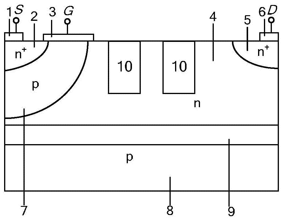
[0043] A pressure-resistant SOI structure based on a folded drift region, such as Figure 6 As shown, the withstand voltage structure at least includes a substrate layer 8, a buried dielectric layer 9 and an active layer 4, and the substrate layer 8, buried dielectric layer 9 and active layer 4 are stacked in sequence from bottom to top. In the present invention, the material of the active layer 4 can be Si, SiC, GaAs, SiGe, GaN or other semiconductor materials. The material of the dielectric buried layer 9 can be SiO 2 Or low-k material, wherein the low-k material (low dielectric constant) can be carbon doped oxide or SiOF, but not limited to the listed materials. The above structure is the basic structure of the existing power devices in the prior art.

[0044] In order to improve the withstand voltage of the SOI device, interdigital dielectric grooves 15 are also provided in the active layer 4 . The interdigitated dielectric groove 15 is composed of at least one downward...

Embodiment 2

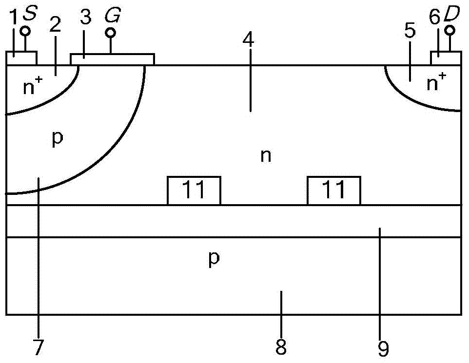
[0050] Another SOI pressure-resistant structure based on the folded drift region, such as Figure 11 As shown, the composition of the pressure-resistant structure, the structure of the interdigitated dielectric groove 15, the material selection of the interdigitated dielectric groove 15, the staggered manner of the downward and upward dielectric grooves, the downward and upward dielectric grooves and the The quantity selection is substantially the same as that in Embodiment 1, the difference being that the dielectric buried layer 9 in Embodiment 1 is a complete laterally extending structure, and completely separates the substrate layer 8 and the active layer 4 vertically. However, in the second embodiment, the buried dielectric layer 9 is provided with a silicon window for heat dissipation, that is, only a part of the buried dielectric layer 12 is provided between the substrate layer 8 and the active layer 4 .

Embodiment 3

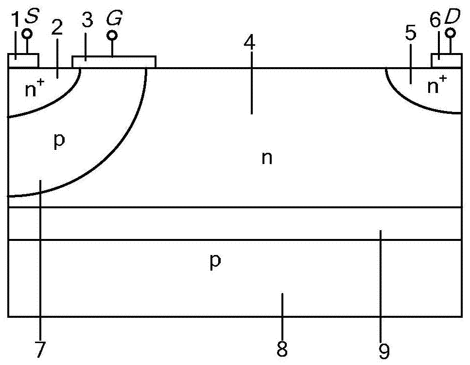
[0052] An SOI power device based on the folded drift region designed based on the SOI voltage-resistant structure of the folded drift region, that is, an SOI LDMOS (lateral double-diffused metal oxide semiconductor) device based on the folded drift region, such as Figure 7 As shown, it includes a substrate layer 8, a dielectric buried layer 9 and an active layer 4 stacked sequentially from bottom to top. An active region 2 , a channel region 7 and a drain region 5 are arranged at upper corners on both sides of the active layer 4 . The source region 2 and the channel region 7 are adjacent to each other, and are arranged at the upper corner of one side of the active layer 4 at the same time. The drain region 5 is disposed at the upper corner of the other side of the active layer 4 . The surface of the active layer 4 is provided with a source electrode 1 , a gate electrode 3 and a drain electrode 6 . The source electrode 1 overlies the source region 2 , and the gate electrode ...


PUM


Abstract

The invention discloses an SOI voltage-resistant structure based on a folded drift region and a power device, including a substrate layer, a dielectric buried layer and an active layer stacked in sequence from bottom to top, and an interdigitated dielectric is also arranged in the active layer groove; the interdigitated dielectric groove is composed of at least one downwardly extending dielectric groove extending downward from the surface of the active layer and at least one upwardly extending dielectric groove extending upwardly from the surface of the dielectric buried layer; wherein the downwardly extending dielectric groove and the upwardly extending dielectric groove The heights are all smaller than the thickness of the active layer, and the downward dielectric grooves and the upward dielectric grooves are arranged alternately in the active layer, and there is a gap between every two adjacent downward dielectric grooves and / or upward dielectric grooves . In the present invention, a plurality of interdigitated dielectric grooves are arranged between the semiconductor active layer and the dielectric buried layer of the power device to improve the lateral and vertical withstand voltages, and significantly improve the blocking characteristics of the device.

Description

technical field [0001] The present invention relates to the technical field of semiconductor power devices and power integration, in particular to an SOI (Silicon On Insulator, silicon on an insulating substrate) withstand voltage structure and power devices used in power devices or high-voltage integrated circuits based on folded drift regions . Background technique [0002] SOI (Silicon On Insulator) power devices have the advantages of high working speed and integration, reliable insulation performance, strong radiation resistance and large safe working area, and are widely used in power electronics, industrial automation, aerospace and weapons Equipment and other fields are the core devices of SOI power integrated circuits. [0003] The structure of a typical conventional n-type SOI LDMOS (Lateral Double Diffused Metal Oxide Semiconductor) device is as follows figure 1 As shown, by the source electrode 1, n+ source region 2, gate electrode 3, n-type active semiconducto...

Claims


Application Information

Patent Timeline
Patent Type & Authority Patents(China)
IPC IPC(8): H01L29/78H01L29/06
CPCH01L29/404H01L29/407H01L29/7824H01L29/0653H01L29/0878
Inventor 李琦李海鸥左园翟江辉
Owner GUILIN UNIV OF ELECTRONIC TECH
Why Eureka
Try Eureka