Method of forming microstructures, laser irradiation device, and substrate

A structural and fine technology, applied in laser welding equipment, electrical connection formation of printed components, manufacturing tools, etc., can solve the ease of etching (different etching speed, longer etching time, excessive etching, etc., to shorten the processing time , Fast etching speed, easy production management

A structural and fine technology, applied in laser welding equipment, electrical connection formation of printed components, manufacturing tools, etc., can solve the ease of etching (different etching speed, longer etching time, excessive etching, etc., to shorten the processing time , Fast etching speed, easy production management

CN102802864AInactive Publication Date: 2012-11-28FUJIKURA LTD

Image

  • Method of forming microstructures, laser irradiation device, and substrate
  • Method of forming microstructures, laser irradiation device, and substrate
  • Method of forming microstructures, laser irradiation device, and substrate

Examples


no. 1 approach

[0105]

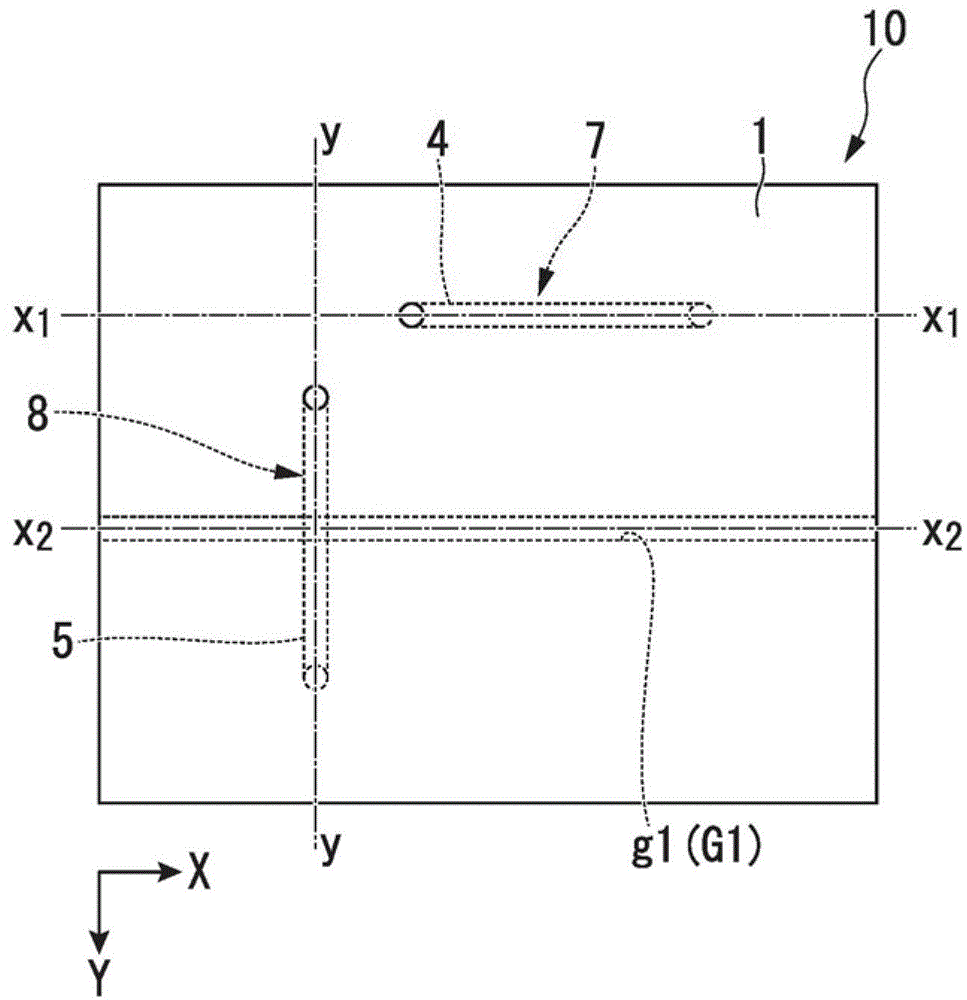
[0106] Figure 1A It is a plan view of interposer substrate 10 according to the first embodiment of the present invention. Figure 1B is along Figure 1A The cross-sectional view of the line x1-x1. Figure 1C is along Figure 1A The cross-sectional view of the y-y line. Figure 1D is along Figure 1A The cross-sectional view of the x2-x2 line.

[0107] The through wiring substrate 10 includes a first through wiring 7 and a second through wiring 8 that connect one main surface 2 (first main surface) and the other main surface 2 (first main surface) of the substrate 1 in a connected manner. The first micropore 4 and the second micropore 5 are arranged so as to form the main surface 3 (second main surface), and the conductive substance 6 is filled or formed into a film in each micropore.

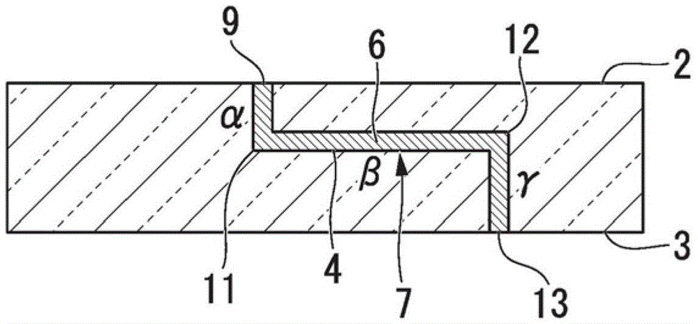
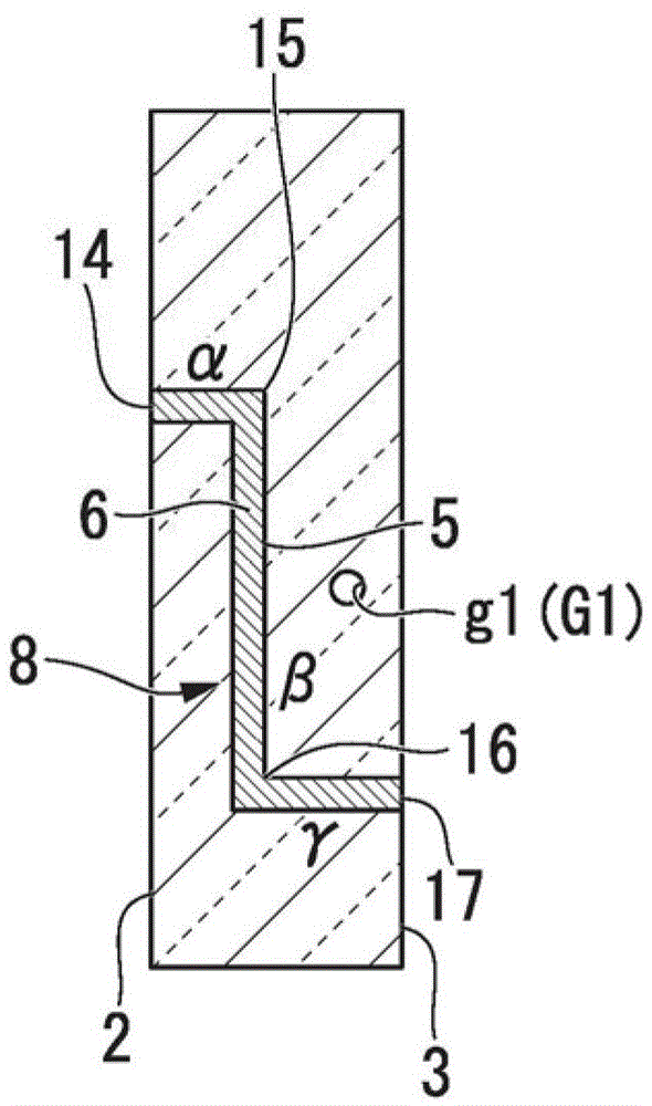
[0108] The first through wiring 7 includes: a region α extending from the opening 9 exposed on the main surface 2 to the bent portion 11 along the thickness direction of the substr...

no. 2 Embodiment approach

[0118]

[0119] Figure 2A It is a plan view of the surface wiring substrate 30 according to the second embodiment of the present invention. Figure 2B is along Figure 2A The cross-sectional view of the line x1-x1. Figure 2C is along Figure 2A The sectional view of the y1-y1 line. Figure 2D is along Figure 2A The cross-sectional view of the x2-x2 line. Figure 2E is along Figure 2A The sectional view of the y2-y2 line.

[0120] This surface wiring substrate 30 is provided with a first surface wiring 37 in which a first microgroove 34 is formed on the surface constituting one main surface 32 (first main surface) of the substrate 31 , and in the microgrooves 34 It is formed by filling or forming a film of a conductive substance 36 . In addition, the surface wiring board 30 is provided with a first flow path G2 constituted by the first fine hole g2 and a second flow path G3 constituted by the second fine hole g3.

[0121] The first surface wiring 37 includes a re...


PUM

PropertyMeasurementUnit
lengthaaaaaaaaaa

Abstract

The disclosed method of forming microstructures involves a step (A) for irradiating, with a laser having a pulse duration on the order of picoseconds or shorter, the region where microstructures configuring holes in a substrate are to be formed and scanning a focus, at which the aforementioned laser is focused, to form a reformed portion, and a step (B) for etching the aforementioned substrate on which the aforementioned reformed portion is formed and removing said reformed portion to form microstructures. In the aforementioned step (A), a linearly polarized laser is used as the aforementioned laser, and said laser is irradiated such that the orientation of the aforementioned linearly polarized light is fixed in direction relative to the scanning direction of the aforementioned focus point.

Description

technical field [0001] The present invention relates to a method of forming a microstructure on a substrate using a laser, a laser irradiation device used in the method, a substrate manufactured by the method, and a substrate having micropores. More specifically, the present invention relates to a method of forming micropores on a substrate using a laser, a laser irradiation device used in the method, a substrate manufactured by the method, and a substrate having the micropores. [0002] This application claims the priority of Japanese Patent Application No. 2010-089509 for which it applied to Japan on April 8, 2010, and uses the content here. Background technique [0003] Conventionally, as a method of electrically connecting a plurality of devices mounted on one main surface and the other main surface of a substrate, a method of forming microscopic holes penetrating between both main surfaces of the substrate and forming microscopic holes near the surface of the substrate ...

Claims


Application Information

Patent Timeline
28 Nov 2012
Publication
CN102802864A
IPC
B23K26/36; B23K26/00; B23K26/04; B23K26/40; H01L23/15; H01L23/52; H05K3/40; H05K3/00; B23K26/046
CPC
H01L2924/0002; H01L23/473; B23K26/365; H05K3/002; B23K26/0635; H05K2203/107; H01L21/4846; B23K26/0042
Inventors
胁冈宽之