Method for transferring Si-based AlGaN/GaN high electron mobility transistor to flexible substrate

A high electron mobility, flexible substrate technology, applied in the direction of circuits, electrical components, semiconductor devices, etc., can solve the problems of slow etching speed and the inability of devices to be used in flexible microelectronic devices, so as to reduce the cost of device transfer and benefit Large-scale flexible semiconductor device production, the effect of thickness reduction

Inactive Publication Date: 2019-08-20
FUDAN UNIV
View PDF5 Cites 8 Cited by
  • Summary
  • Abstract
  • Description
  • Claims
  • Application Information

AI Technical Summary

Problems solved by technology

The disadvantage of this technology is that it needs to use hydrofluoric acid wet etching to remove the Si substrate of the device, and the etching speed is slow; and after the device is transferred to the quartz substrate, due to the high hardness of quartz, there is no flexibility. devices cannot be used as flexible microelectronics

Method used


Image

  • Method for transferring Si-based AlGaN/GaN high electron mobility transistor to flexible substrate
  • Method for transferring Si-based AlGaN/GaN high electron mobility transistor to flexible substrate
  • Method for transferring Si-based AlGaN/GaN high electron mobility transistor to flexible substrate

Examples


Embodiment Construction

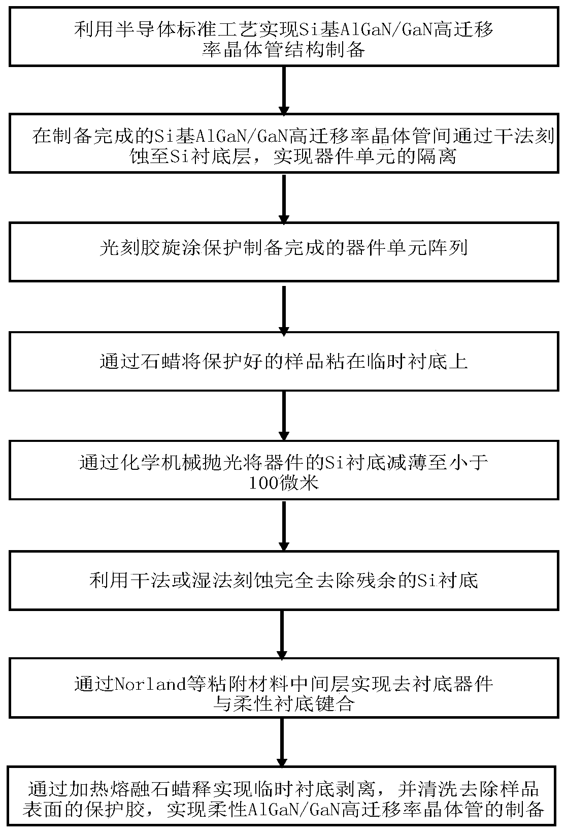
[0048]The present invention will be described in further detail below in conjunction with specific examples, which are further explanations of the present invention rather than limitations.

[0049] The invention provides a method for fabricating a Si-based AlGaN / GaN high electron mobility transistor and realizing a flexible substrate, which specifically includes the following steps.

[0050] Step 1: The thickness of the Si substrate 100 is 800 microns, the thickness of the GaN high-resistance buffer layer 110 is 3.5 microns, the thickness of the GaN layer 120 is 100 nm, the thickness of the AlGaN layer 130 is 20 nm, and the Al composition is 0.25. 20nm SiN grown by LPCVD X The thin film 200 is used as the gate dielectric of the device, and the source-drain ohmic contact electrode 210 of the device is made of four metal combinations of Ti / Al / Ni / Au, and then heated at 870°C and N 2 Rapid annealing under atmosphere for 30 seconds, the gate metal 220 uses Ni / Au electrodes.

[0...


PUM


Abstract

The invention belongs to the technical field of semiconductors and particularly relates to a method for transferring a Si-based AlGaN/GaN high electron mobility transistor to a flexible substrate. Themethod of the invention comprises a step of achieving the stripping of a non-flexible Si substrate by using a mode of combining chemical mechanical polishing and dry or wet etching, and a step of transferring the high electron mobility transistor device with the removal of a substrate to the flexible substrate through an intermediate layer of an adhesive material such as Norland by using a devicebonding technique to achieve the preparation of the AlGaN/GaN high electron mobility transistor. The method has the advantages of fast etching speed, low process cost and wide application range, andthe invention includes but not limited to a hard substrate semiconductor device based on a Si substrate or a sapphire substrate.

Description

technical field [0001] The invention belongs to the technical field of semiconductors, and in particular relates to a method for transferring a Si-based AlGaN / GaN high electron mobility transistor to a flexible substrate. Background technique [0002] With the increasing demand for various applications of flexible electronics, it is required to develop devices with higher performance while maintaining the basic requirements of mechanical flexibility and thinness. Organic semiconductors and amorphous semiconductor materials have been widely used in flexible electronics. However, the performance improvement and application expansion of these devices are limited due to the low mobility and low operating temperature of organic materials. However, the application power and operating temperature requirements can be extended by developing flexible devices based on novel semiconductor materials. Wide bandgap Ⅲ-nitride (Ⅲ-Ⅴ) materials have broad application prospects in flexible el...

Claims


Application Information

Patent Timeline
Patent Type & Authority Applications(China)
IPC IPC(8): H01L21/335
CPCH01L29/66462
Inventor 田朋飞赵德胜林润泽刘冉郑立荣
Owner FUDAN UNIV
Why Eureka
Try Eureka