Simple and easy preparation method of nanometer-scale PPS (Patterned Sapphire Substrate)

A nano-scale, substrate technology, applied in electrical components, circuits, semiconductor devices, etc., can solve the problems of complex processing and high cost, and achieve the effects of reduced processing costs, fast etching speed, and low technical requirements.

Active Publication Date: 2012-03-07
HC SEMITEK CORP
View PDF6 Cites 8 Cited by
  • Summary
  • Abstract
  • Description
  • Claims
  • Application Information

AI Technical Summary

Problems solved by technology

[0003] At present, the nano-scale PPS substrate technology mainly adopts: electron beam lithography technology, nanoimprint lithography technology, polymer lithography technology; the above technologies are complicated to process and high in cost

Method used


Image

  • Simple and easy preparation method of nanometer-scale PPS (Patterned Sapphire Substrate)
  • Simple and easy preparation method of nanometer-scale PPS (Patterned Sapphire Substrate)

Examples


Embodiment 1

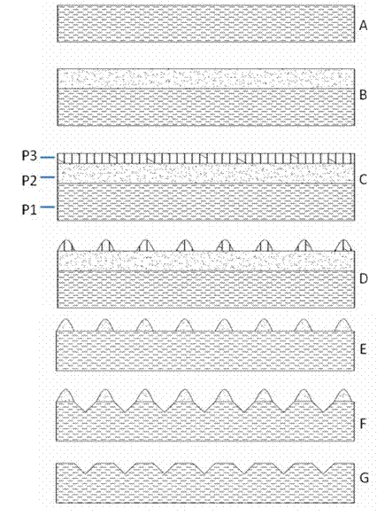
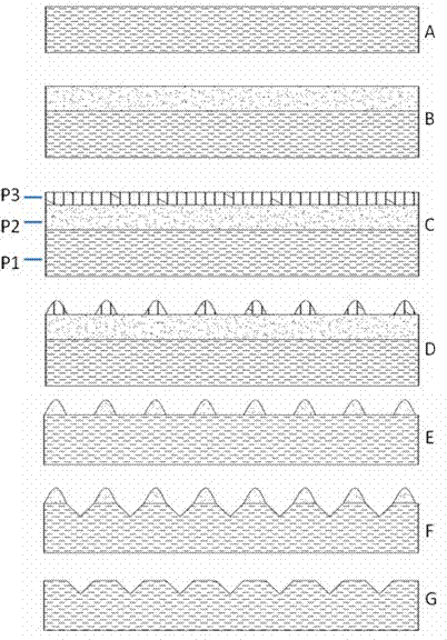
[0023] First deposit a layer of SiO2 film on the sapphire substrate with PECVD equipment, with a thickness of about 2000-5000 angstroms;

[0024] Then deposit a layer of ITO or ZnO film on the SiO2 film with a thickness of about 1000-3000 angstroms; anneal the ITO or ZnO film at a temperature of 300-600 ° C for 0.5-2 hours to form a uniform ITO or ZnO film on the surface of the SiO SiO2 film. ZnO grains (80-300 angstroms); then use RIE equipment (parameters: CF4: 30-60sccm; reaction pressure: 20-100mTorr; power: 300-500W, etching time: 10-30 minutes), then use sulfuric acid and Phosphoric acid mixing volume ratio: 3:1; etch in the mixed solution at temperature (230-350°C) for 10-30 minutes; finally use HF acid to etch the SiO2 mask for 10-30 minutes.


PUM

PropertyMeasurementUnit
thicknessaaaaaaaaaa

Abstract

The invention relates to a simple and easy preparation method of a nanometer-scale PPS, comprising the following steps of: depositing an SiO2 film on a sapphire substrate; depositing an ITO (Indium Tin Oxide) or ZnO layer on the SiO2 film; carrying out high-temperature annealing to enable the ITO or ZnO film to undergo an agglomeration phenomenon, wherein the size and the distributive degree of ITO or ZnO particles on the SiO2 film are changed according to the annealing temperature; etching the SiO2 film which is blocked by the ITO or ZnO particles off through dry etching, thereby transferring a uniform ITO or ZnO nanoparticle pattern to the SiO2 film; then putting the SiO2 film to a high-temperature mixed solution containing sulfuric acid and phosphoric acid for corroding or dry etching; transferring the uniform nanometer-scale SiO2 particle pattern to the sapphire substrate again; and finally removing an SiO2 mask film with HF acid to form the nanometer-scale PSS substrate. The simple and easy preparation method disclosed by the invention has the advantages of simple and easy preparation process, low cost, high production efficiency and capability of improving the quantum effect outside an LED chip.

Description

technical field [0001] The invention relates to a method for manufacturing an LED substrate, in particular to a method for preparing a simple nanoscale PSS substrate. Background technique [0002] Light-emitting diode (LED) is a kind of electro-optic conversion, high efficiency and energy saving, green environmental protection, long life, etc. Solid-state lighting, which is expected to become a new generation of light source and enter thousands of households, will cause a revolution in the history of human lighting. Among them, the blue LED chip grown on the sapphire substrate with gallium nitride epitaxy is coated with yellow light phosphor, and the blue light excites the phosphor to emit yellow light. Blue light is mixed with yellow light to get white light, so blue LEDs are used to get white light. There are two common gallium nitride substrate materials, namely sapphire and silicon carbide. The poor machining performance of silicon carbide, high price and patent issues ...

Claims


Application Information

Patent Timeline
Patent Type & Authority Applications(China)
IPC IPC(8): H01L33/00
Inventor 周武罗红波张建宝刘榕
Owner HC SEMITEK CORP
Why Eureka
Try Eureka