A/D converter input stage

An analog-to-digital converter, input stage technology, applied in the direction of analog-to-digital converter, analog conversion, code conversion, etc., can solve problems such as increasing noise

Active Publication Date: 2015-06-24
NXP BV
View PDF3 Cites 3 Cited by
  • Summary
  • Abstract
  • Description
  • Claims
  • Application Information

AI Technical Summary

Problems solved by technology

The disadvantage of this implementation is that both transconductance elements have to convert the full-swing signal (either the input signal or the DA converter output signal), which requires a higher linearity level to avoid disto

Method used


Image

  • A/D converter input stage
  • A/D converter input stage
  • A/D converter input stage

Examples


Embodiment Construction

[0047] The examples in the figures are schematic. It should be noted that in different drawings, similar or identical components in various embodiments are represented by identical or similar symbols, and only the first number changes.

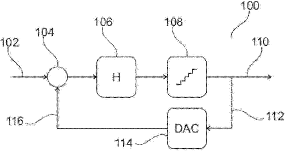
[0048] about figure 1 and figure 2 , as a reference to the corresponding description given above.

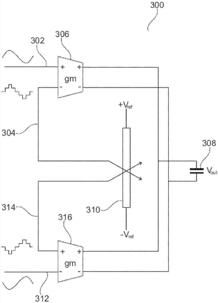
[0049] image 3 A schematic diagram of an input stage for a differential analog-to-digital converter according to an embodiment of the invention is shown.

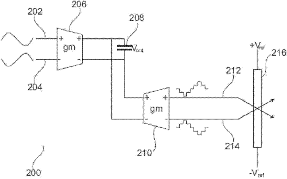
[0050] Typically, the input stage 300 is structured with figure 2 The input stage 200 of the known art shown differs in that each transconductance element of the input stage 300 receives an analog input signal and an analog feedback signal having the same polarity, so that each transconductance element of the input stage 300 is more than figure 2 The transconductance element of the known art input stage 200 experiences less signal swing.

[0051] More specifically, as image 3 As s...


PUM


Abstract

There is described an input stage for an A/D converter, comprising (a) a transconductance element (306, 406) adapted to receive, at a first input (302, 402) of the transconductance element, an analog input signal that is to be converted to a digital signal by the A/D converter, (b) a feedback path for providing an analog feedback signal to a second input (304, 404) of the transconductance element, the analog feedback signal being based on a digital output signal of the A/D converter, and (c) an integrator (308, 408) for integrating an output current of the transconductance element, wherein the integrating element is adapted to generate an integrator output signal representative of the integrated output current. There is also described an A/D converter comprising such an input stage and a system comprising a plurality of such A/D converters.

Description

technical field [0001] The present application relates to the field of analog-to-digital converters, in particular input stages for such converters. Background technique [0002] In an A / D converter (analog-to-digital converter), the input stage is usually the most critical part of the converter related to noise and linearity. To improve linearity, degeneration of the input transistor pair is often used, but this also increases noise. Another solution is to use an input stage that has feedback to the input of the amplifier (like an inverting amplifier), but requires an input resistor, so the input impedance of the A / D converter will be limited, but this is not Desirable, especially undesirable when an A / D converter needs to interface with a sensor. Also, this feedback increases power consumption. [0003] Additionally, in sensor applications, it is often required that the signal processing path provide sufficient gain matching between the different channels. For example,...

Claims


Application Information

Patent Timeline
IPC IPC(8): H03M1/12
CPCH03M3/35H03M3/424H03M1/12
Inventor 罗伯特·H·M·范费尔德温法比奥·塞巴斯蒂亚诺
Owner NXP BV
Why Eureka
Try Eureka