Structure and manufacturing method of mask type read-only memory

A read-only memory and manufacturing method technology, applied in semiconductor/solid-state device manufacturing, semiconductor devices, electric solid-state devices, etc., can solve the problems of poor device uniformity, high process cost, large injection energy, etc., to ensure process uniformity, The effect of stable difference value and lower manufacturing cost

Active Publication Date: 2019-01-04
SHANGHAI HUAHONG GRACE SEMICON MFG CORP
View PDF3 Cites 0 Cited by
  • Summary
  • Abstract
  • Description
  • Claims
  • Application Information

AI Technical Summary

Problems solved by technology

Since this implantation must pass through the polysilicon gate, the implantation energy required is relatively large, and the impurity loss during the implantation process is relatively large.
Therefore, devices with high threshold voltages have poor uniformity, resulting in a smaller space between information "0" and "1"
In addition, the writing of the code also requires an additional photomask and a separate photolithography and ion implantation process, so the process cost is relatively high

Method used


Image

  • Structure and manufacturing method of mask type read-only memory
  • Structure and manufacturing method of mask type read-only memory
  • Structure and manufacturing method of mask type read-only memory

Examples


Embodiment Construction

[0021] In order to have a more specific understanding of the technical content, characteristics and effects of the present invention, now in conjunction with the accompanying drawings, the details are as follows:

[0022] The manufacturing method of mask type read-only memory of the present invention, its concrete processing steps are as follows:

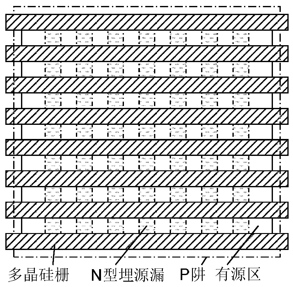
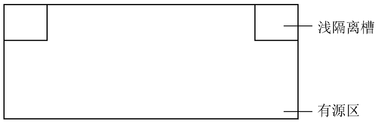
[0023] Step 1, forming shallow isolation trenches on the active area of ​​the silicon substrate to isolate the mask-type read-only memory area from peripheral circuits, such as image 3 shown.

[0024] Step 2, perform P well implantation in the active area of ​​the mask type ROM to form the active area in the P well, such as Figure 4 (Figure B is the top view after this step is completed).

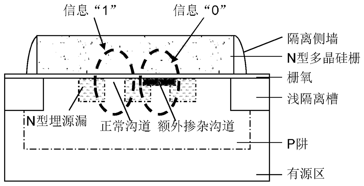
[0025] Step 3, coating N-type buried source and drain photoresist, exposing, and then performing a high-dose arsenic ion or phosphorus ion implantation with low energy to form N-type buried source and drain, such as Figure 5 shown.

[0026...


PUM


Abstract

The invention discloses a method for manufacturing a photomask type read-only memory. The steps include: 1) forming a shallow isolation groove and performing P well implantation; 2) forming an N-type buried source and drain; 3) forming a polysilicon gate and a first isolation side wall and the second isolation spacer; 4) perform source-drain implantation on NMOS, and perform N-type doping on the area of ​​information unit "1" at the same time; Perform P-type doping; 6) Form metal silicide on the polysilicon gate to complete the fabrication of the mask-type read-only memory. In the present invention, by changing the code writing method and device structure of the mask-type read-only memory, the information unit "1" adopts an N-type polysilicon gate, and the information unit "0" adopts a P-type polysilicon gate. Since the N-type and P-type polysilicon gates The difference of the threshold voltage is only about 1.12eV, and the difference is stable, so that the writing of information "0" can be realized, and the uniformity of the device is guaranteed.

Description

technical field [0001] The invention relates to the field of integrated circuit manufacturing, in particular to the structure and manufacturing method of a mask type read-only memory. Background technique [0002] Read-Only Memory (Read-Only Memory) is a memory that can only read data. The data of this memory is written at the time of production. In the manufacturing process, the data is burned into the circuit with a special mask (mask), so it is sometimes called "mask ROM" (mask ROM). In fact, it is very similar to the principle of a CD disc, in which the data state is written in the photolithography process of the semiconductor. [0003] The data of this mask-type read-only memory cannot be changed after writing, so the data cannot be lost, and its manufacturing cost is very low. Therefore, in devices that do not require data update, Mask ROM is very widely used use. [0004] In order to achieve as high a device density as possible in a traditional mask-type read-only...

Claims


Application Information

Patent Timeline
Patent Type & Authority Patents(China)
IPC IPC(8): H01L21/8246H01L27/112
CPCH10B20/34
Inventor 刘冬华钱文生
Owner SHANGHAI HUAHONG GRACE SEMICON MFG CORP
Why Eureka
Try Eureka