Reaction chamber and semiconductor processing equipment

A reaction chamber and chamber wall technology, which is applied in semiconductor devices, semiconductor/solid-state device manufacturing, electric solid-state devices, etc., can solve the problems of non-axial sidewalls, exceeding component variation, and breaking of ceramic rings 109, etc. Achieve the effect of improving process stability and equipment reliability, improving process uniformity, and ensuring process uniformity

Active Publication Date: 2020-02-14
BEIJING NAURA MICROELECTRONICS EQUIP CO LTD
View PDF7 Cites 0 Cited by
  • Summary
  • Abstract
  • Description
  • Claims
  • Application Information

AI Technical Summary

Problems solved by technology

However, when a new target is cleaned to remove oxides and pollutants on its surface, the temperature of the Faraday shielding ring 108 will rise significantly (over 300° C.) due to continuous bombardment. At this time, the diameter of the Faraday shielding ring 108 The amount of expansion is about 3mm, which exceeds the allowable variation of components, which may cause the ceramic ring 109 to be broken
In addition, the distance between the screw 110 and the ceramic ring 109 is not allowed to exceed 1.5 mm, otherwise the accurate positioning of the Faraday shielding ring 108 cannot be ensured, resulting in the problem that the Faraday shielding ring 108 and the side wall of the reaction chamber 101 are out of alignment. , affecting the final process result

Method used


Image

  • Reaction chamber and semiconductor processing equipment
  • Reaction chamber and semiconductor processing equipment
  • Reaction chamber and semiconductor processing equipment

Examples


Embodiment Construction

[0034] In order for those skilled in the art to better understand the technical solution of the present invention, the reaction chamber and semiconductor processing equipment provided by the present invention will be described in detail below in conjunction with the accompanying drawings.

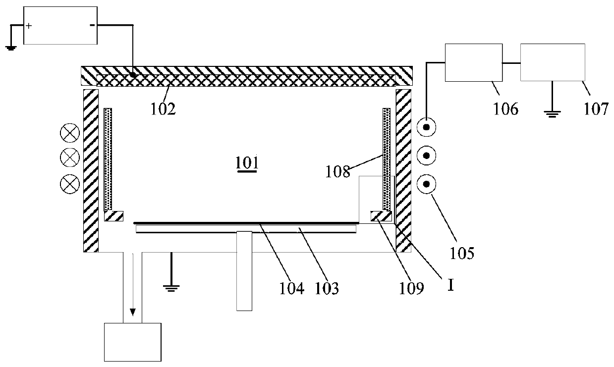
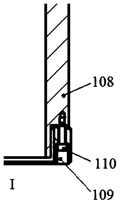
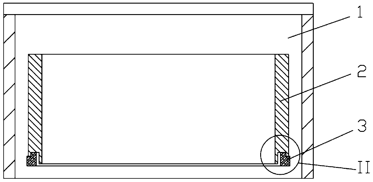
[0035] image 3 A cross-sectional view of a reaction chamber provided for an embodiment of the present invention. see image 3 , the reaction chamber 1 includes a Faraday shielding ring 2 and an insulating ring 3 . Among them, when the reaction chamber 1 is used in the metal deposition process, it is easy to form a metal shield on the inner wall of the chamber using an insulating medium, causing electromagnetic energy to be shielded outside the chamber. For this reason, through the reaction chamber 1 A Faraday shielding ring 2 is arranged around the inner side of the side wall to ensure that radio frequency energy is smoothly coupled into the reaction chamber 1 through the radio frequency...


PUM

PropertyMeasurementUnit
widthaaaaaaaaaa

Abstract

The invention provides a reaction chamber and a semiconductor processing device. The reaction chamber includes a Faraday shielding ring and an insulation ring used for supporting the Faraday shieldingring, a support surface of the insulation ring is provided with a concave part, a supported surface of the Faraday shielding ring is provided with a convex part, the convex part is positioned in theconcave part, the concave part includes a first side face facing the outside direction, the convex part includes a second side face facing the inner direction, and the first side surface and the second side surface are attached to each other; and the concave part is arranged in such a manner that the convex part is not restricted by the concave part when heated and expanded. The reaction chamber has the advantages that the insulation ring cannot be damaged at high temperature, the precise positioning of the Faraday shielding ring can be guaranteed, and the uniformity and stability of the technology and the reliability of the device can be improved.

Description

technical field [0001] The invention relates to the field of semiconductor manufacturing, in particular to a reaction chamber and semiconductor processing equipment. Background technique [0002] With the development of Moore's Law, in the production of semiconductor processing equipment for VLSI, it is often necessary to coat structures with high aspect ratios, such as channels, trenches and vias, which can increase the plasma in the reaction chamber. In order to obtain better deep hole deposition ability. In order to increase the specific gravity of ions in the chamber, the existing semiconductor processing equipment adds radio frequency coils around the reaction chamber to couple electromagnetic energy into the reaction chamber, thereby increasing the specific gravity of ions and obtaining good process performance . [0003] In the metal deposition reaction chamber, it is easy to form a metal shield on the inner wall of the chamber using an insulating medium, causing el...

Claims


Application Information

Patent Timeline
Patent Type & Authority Patents(China)
IPC IPC(8): H01J37/32H01L21/67
CPCH01J37/32431H01J2237/026H01L21/67017H01L2221/67H01L2221/683
Inventor 佘清张彦召赵梦欣
Owner BEIJING NAURA MICROELECTRONICS EQUIP CO LTD
Why Eureka
Try Eureka