
Semiconductor processing equipment

A technology for processing equipment and semiconductors, which is applied in semiconductor/solid-state device manufacturing, metal material coating process, coating, etc., and can solve problems such as gas composition changes and process uniformity effects.

Active Publication Date: 2019-08-23
BEIJING NAURA MICROELECTRONICS EQUIP CO LTD
View PDF4 Cites 0 Cited by
  • Summary
  • Abstract
  • Description
  • Claims
  • Application Information

AI Technical Summary

Problems solved by technology

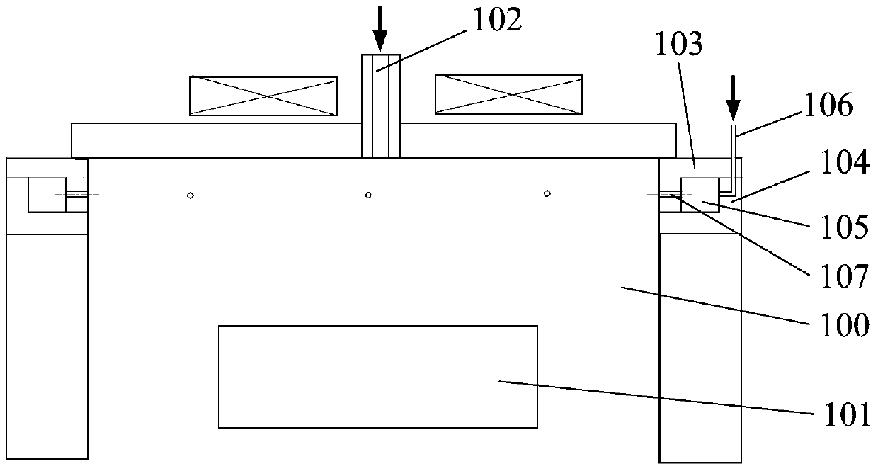
[0005] However, for the edge inlet mechanism, after it completes the delivery of the second process gas, a part of the process gas will remain in the inside of the uniform flow chamber 105, and when the edge inlet mechanism is not used, due to the uniform flow chamber 105 Each gas outlet 107 is always in communication with the reaction chamber 100, which makes the second process gas remaining in the uniform flow chamber 105 enter the reaction chamber 100 and mix with the first process gas, resulting in the reaction chamber The composition of the gas within 100 changes, which affects the uniformity of the process

Method used


Image

  • Semiconductor processing equipment
  • Semiconductor processing equipment
  • Semiconductor processing equipment

Examples


Embodiment Construction

[0027] In order for those skilled in the art to better understand the technical solutions of the present invention, the semiconductor processing equipment provided by the present invention will be described in detail below in conjunction with the accompanying drawings.

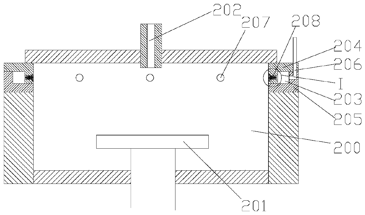
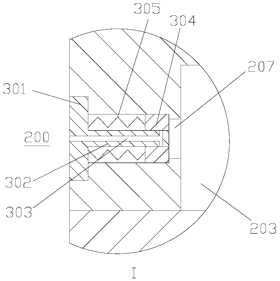
[0028] Figure 2A It is a cross-sectional view of the semiconductor processing equipment provided by the first embodiment of the present invention. see Figure 2A , the semiconductor processing equipment includes a reaction chamber 200, a central inlet mechanism 202 and an edge inlet mechanism, wherein a chuck 201 for carrying a workpiece to be processed is arranged in the reaction chamber 200. The central air inlet mechanism 202 is arranged at the center of the top of the reaction chamber 200 . The edge air inlet mechanism includes an air inlet 206, a uniform flow chamber 203 and a plurality of gas outlets 207, wherein the uniform flow chamber 203 is spliced ​​by two surrounding cover plates (204, 205) arra...


PUM


Abstract

The semiconductor processing equipment provided by the present invention includes a reaction chamber, a central air inlet mechanism and an edge air inlet mechanism, wherein the central air inlet mechanism is arranged at the top center of the reaction chamber; the edge air inlet mechanism includes an air inlet, a uniform A flow chamber and multiple gas outlets, the uniform flow chamber is arranged around the edge of the reaction chamber; the multiple gas outlets are evenly distributed along the circumference of the uniform flow chamber. An on-off device is provided in each gas outlet to make the gas outlet communicate with the reaction chamber under the action of air pressure when the process gas is delivered to the uniform flow chamber through the inlet; When the process gas is transported in the chamber, the gas outlet is isolated from the reaction chamber under the action of air pressure. The semiconductor processing equipment provided by the present invention can prevent the process gas remaining in the uniform flow chamber from entering the reaction chamber when two different process gases are alternately fed into the reaction chamber, thereby ensuring process uniformity.

Description

technical field [0001] The present invention relates to the field of semiconductor manufacturing, in particular to a semiconductor processing equipment. Background technique [0002] Plasma processing equipment is widely used in the manufacturing process of integrated circuits (IC) or MEMS devices. It uses a large number of active particles such as electrons, ions, and excited atoms to undergo various physical and chemical reactions with the surface of the substrate. Thus, the properties of the substrate surface are changed. In the manufacturing process of integrated circuits, an air intake mechanism is usually used to provide a gas source for generating plasma. [0003] figure 1 It is a structural schematic diagram of the existing plasma processing equipment. see figure 1 , the plasma processing equipment includes a reaction chamber 100 and an inlet device, wherein a chuck 101 for carrying a substrate is arranged in the reaction chamber 100 . The air intake device incl...

Claims


Application Information

Patent Timeline
Patent Type & Authority Patents(China)
IPC IPC(8): H01L21/67
CPCH01L21/67011C23C16/4409C23C16/4412C23C16/45502H01J37/32449H01L21/67017H01L21/6719C23C16/4558H01L21/677
Inventor 赵隆超
Owner BEIJING NAURA MICROELECTRONICS EQUIP CO LTD
Learn More