Touch panel liquid crystal display

a liquid crystal display and touch panel technology, applied in the direction of electric digital data processing, instruments, computing, etc., can solve the problems of large volume of aluminum foil or conductive spongy mentioned above, non-operational products, and inability to release electrostatic charges generated during the panel manufacturing process or transferred from users to the touch panel. to achieve the effect of increasing the conducting rate of the transparent conducting layer

Inactive Publication Date: 2005-03-10
INNOLUX CORP
View PDF5 Cites 141 Cited by
  • Summary
  • Abstract
  • Description
  • Claims
  • Application Information

AI Technical Summary

Benefits of technology

[0012] In brief, the touch panel of the present invention uses a transparent conducting layer and a conducting buffer material to conduct the electrostatic charges generated in the touch control panel of the touch panel liquid crystal display to ground. The path to ground can be through the casing electrically connected to ground or through the conducting casing of the LCD module. Further, the conducting buffer material of the present invention can be conducting rubber or conducting rubber with copper threads or steel threads to increase the conducting rate of the transparent conducting layer. Hence, the present invention can effectively release the electrostatic charges from the touch panel and prevent the electrostatic charges entering into the controlling circuit board and the other electronic devices in the LCD.

Problems solved by technology

Although the touch panel manufacturing process is quite mature, the electrostatic charges generated during the panel manufacturing process or transferred from users to the touch panel may not be released from the touch panel after the touch panel and the LCD module are assembled into the LCD device.
In other words, the electrostatic charges generated during the panel manufacturing process or transferred from users to the touch panel are conducted directly to the controlling circuit board or other data processing devices to induce damages to other electrical devices which cause the product non-operational.
However, the volume of the aluminum foil or conductive spongy mentioned above is quite large in size.

Method used


Image

  • Touch panel liquid crystal display
  • Touch panel liquid crystal display
  • Touch panel liquid crystal display

Examples


Embodiment Construction

[0028] The following description is of the best-contemplated mode of carrying out the invention. This description is made for the purpose of illustrating the general principles of the invention and should not be taken in a limiting sense. The scope of the invention is best determined by reference to the appended claims.

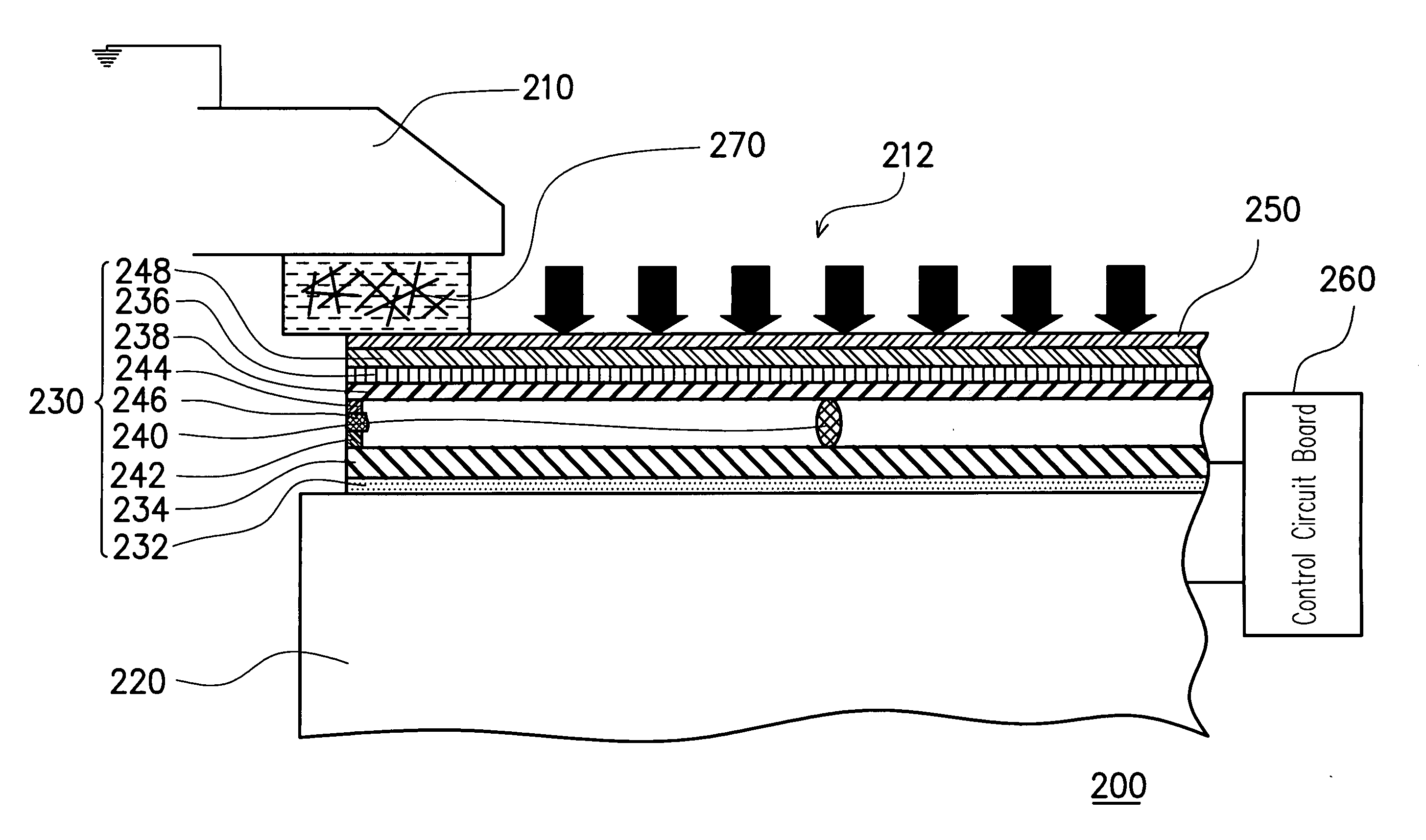
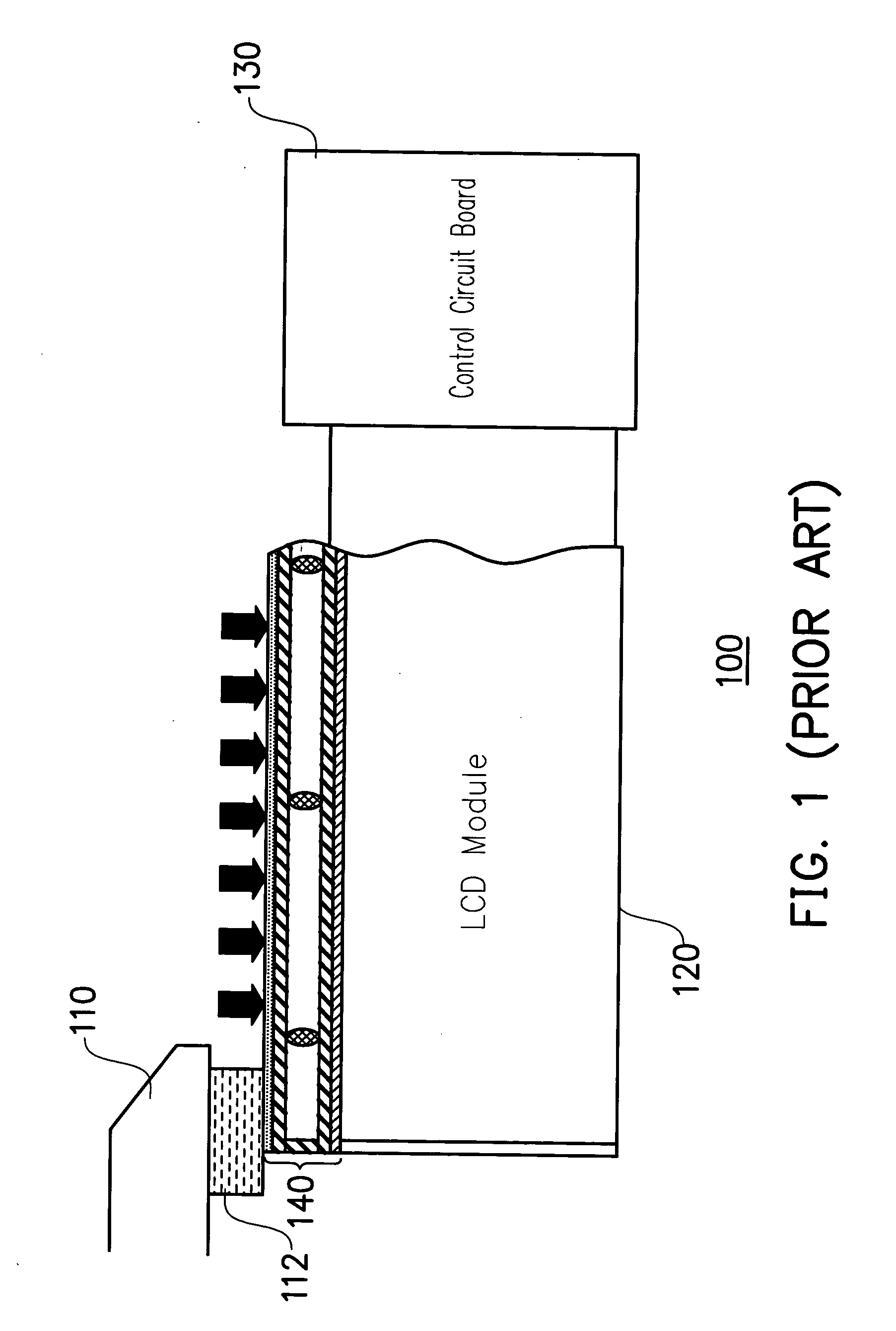
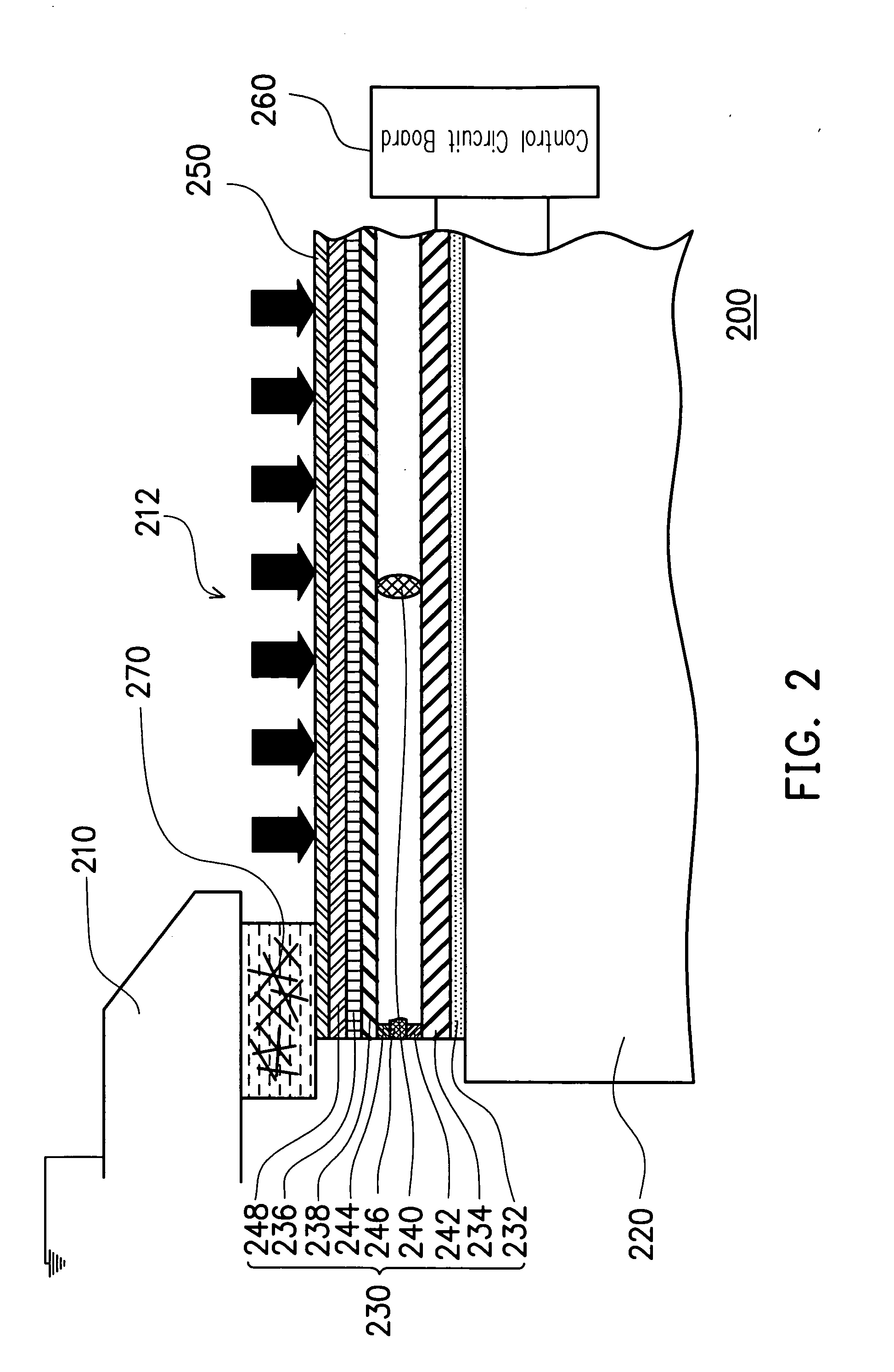
[0029] It is noted that the description hereinbelow refers to various layers arranged on, above or overlying other layers, to describe the relative positions of the various layers. References to “on”, “above”, “overlying”, or other similar languages, are not limited to the interpretation of one layer being immediately adjacent another layer. There may be intermediate or interposing layers, coatings, or other structures present, and associated process steps present, which are not shown or discussed herein, but could be included to accomplish the intended purpose without departing from the scope and spirit of the invention disclosed herein. Similar, references to struc...


PUM

PropertyMeasurementUnit
transparentaaaaaaaaaa
conductingaaaaaaaaaa
non-conductingaaaaaaaaaa

Abstract

A touch-panel liquid crystal display is provided. The touch-panel liquid crystal display comprises a casing, a liquid crystal display module, a touch panel, a transparent conducting layer, a controlling circuit board, and a conductive buffer layer. The transparent conducting layer is disposed on the surface of the touch panel. The conductive buffer layer is disposed between the casing and the transparent conducting layer. The conductive buffer layer can be electrically connected to the casing or the conductive module casing of the liquid crystal display module so that the electrostatic charges can be released from the touch-panel LCD to ground. Hence, the electrostatic charges are effectively released from the touch panel and are prevented from entering into the controlling circuit board and the other electronic devices in the LCD.

Description

CROSS-REFERENCE TO RELATED APPLICATION [0001] This application claims the priority benefit of Taiwan application serial no. 92124835, filed on Sep. 9, 2003. BACKGROUND OF THE INVENTION [0002] 1. Field of the Invention [0003] This invention generally relates to a touch panel liquid crystal display, and more particularly to a touch panel liquid crystal display with electrostatic discharge protection. [0004] 2. Description of Related Art [0005] As technology advances, digital devices such as mobile phones, PDAs, notebook computers, and tablet computers are developed to provide convenience, versatility and attractive appearances. The displays for these devices thus become indispensable interfaces between the users and the devices. Among the various types of displays, liquid crystal display (LCD) becomes the main stream for these digital devices. [0006] Recently, to facilitate the users' input, many digital devices have adopted touch panel LCD as the inputting device rather than traditio...

Claims


Application Information

Patent Timeline
Patent Type & Authority Applications(United States)
IPC IPC(8): G02F1/133G06F1/16G06F3/033G06F3/041
CPCG02F1/13338G02F2202/22G06F3/041G06F1/1637G06F3/03547G06F1/1626
Inventor MAI, CHE-KUEI
Owner INNOLUX CORP
Why Eureka
Try Eureka