Peeling method

a peeled layer and peeled technology, applied in the direction of semiconductor devices, electrical apparatus, transistors, etc., can solve the problems of difficult cracks and heavyness, inability to form any tft with electric characteristics, and difficult enlargement of glass substrates, etc., to and promote deterioration of organic compound layers

Inactive Publication Date: 2006-10-17
SEMICON ENERGY LAB CO LTD
View PDF52 Cites 141 Cited by
  • Summary
  • Abstract
  • Description
  • Claims
  • Application Information

AI Technical Summary

Benefits of technology

[0010]The invention has been completed in consideration of the above-described problems and the invention aims to provide a peeling method without damaging a layer to be peeled and to allow separation of not only a layer to be peeled having a small surface area but also the entire surface of a layer to be peeled having a large surface area.
[0013]Through a large number of experiments and examinations, the inventors of the present invention have found a peeling method in which, when: a metal layer is provided on a substrate; an oxide layer is formed contacting with the metal layer; an insulating film is formed on the oxide layer; a layer containing hydrogen, typically an amorphous silicon film containing hydrogen, is formed on the insulating film; and heat treatment is performed to the resultant lamination layer at 410° C. or more, while abnormality in the process such as peeling does not occur, peeling can be completely performed with ease at an interface of the oxide layer (interface of the oxide layer and the metal layer) by using physical means, typically performing application of a mechanical force (for example, performing peeling with hand).
[0015]Further, when the oxide layer is formed on the metal layer, a surface of the metal layer is oxidized. Thus, adhesion property between the metal layer and the oxide layer is improved. Then, it is considered that hydrogen contained in the layer containing hydrogen is diffused at 410° C. or more, and the reaction (for example, reduction reaction) of hydrogen and the oxidized surface of the metal layer occurs, whereby the adhesion property between the metal layer and the oxide layer is lowered. In addition, since the stress of the layer containing hydrogen is changed toward a tensile stress through heating, distortion is caused at the interface of the metal layer and the oxide layer, which easily leads to peeling.
[0051]Further, in each of the above-described structures related to the method of manufacturing a semiconductor device, in the case of the manufacture of a light emitting device typified as a light emitting device including an EL element, it is preferable that: the support member is used as a sealing member; and a light emitting element is completely shut off from the outside to avoid the entry of a substance which promotes deterioration of an organic compound layer, such as moisture or oxygen from the outside. Further, when reduction in weight is placed at the highest priority, a film-like plastic substrate is preferably used. However, this exerts a little effect of avoiding the entry of the substance, which promotes deterioration of the organic compound layer, such as moisture or oxygen from the outside. Therefore, there may be adopted, for example, a structure in which a first insulating film, a second insulating film, and a third insulating film are provided on the support member, thereby sufficiently avoiding the entry of the substance which promotes deterioration of the organic compound layer, such as moisture or oxygen from the outside. Note that the second insulating film (stress relaxing film) sandwiched between the first insulating film (barrier film) and the third insulating film (barrier film) is made to have a film stress smaller than that of either the first insulating film or the third insulating film.
[0052]Moreover, in the case of the manufacture of a light emitting device typified as a light emitting device including an EL element, it is preferable that a first insulating film, a second insulating film, and a third insulating film are provided to not only the support member but also the transfer member, which sufficiently avoids the entry of the substance which promotes deterioration of the organic compound layer, such as moisture or oxygen from the outside.

Problems solved by technology

Today, although a glass substrate, a quartz substrate and the like are used in many cases, they have disadvantages that they are easy to crack and heavy.
Further, in terms of mass production, the glass substrate, the quartz substrate and the like are difficult and unsuitable for enlargement.
However, since the heat resistance of the plastic film is low, the highest temperature for process is required to be low and consequently, it is presently impossible to form any TFT with electric characteristics as excellent as those formed on a glass substrate.
In order to transmit energy through the substrate and supply energy sufficient to release hydrogen contained in the amorphous silicon, relatively intense laser beam has to be radiated, resulting in a problem that the layer to be peeled is damaged.
As a result, there is a possibility of insufficient peeling, even if laser beam is radiated to the isolation layer.
Subsequently, attributed to retention of the quantity of hydrogen contained in the isolation layer, there occurs a problem that the process after isolation layer formation may be limited.
In such a case, it becomes difficult to fabricate a transmission type liquid crystal display device.
Additionally, by the above-described method, peeling of the layer to be peeled having a large surface area becomes difficult.

Method used


Image

  • Peeling method
  • Peeling method
  • Peeling method

Examples


experiment 1

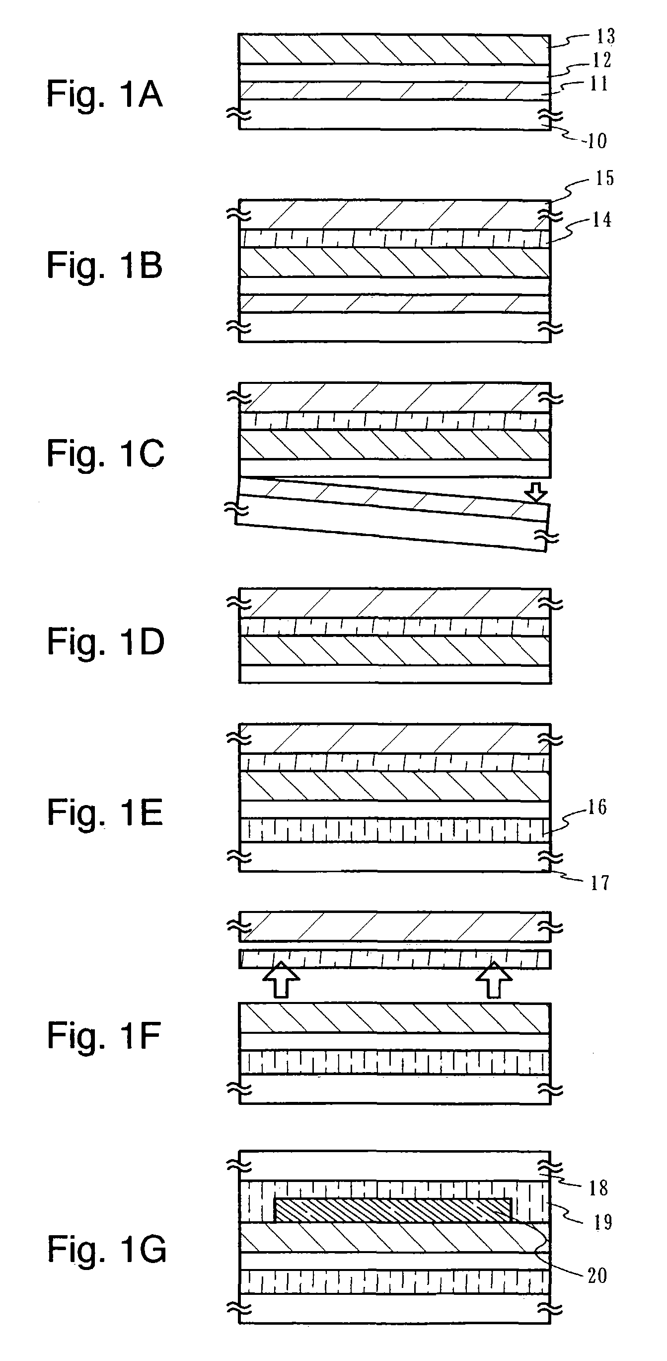
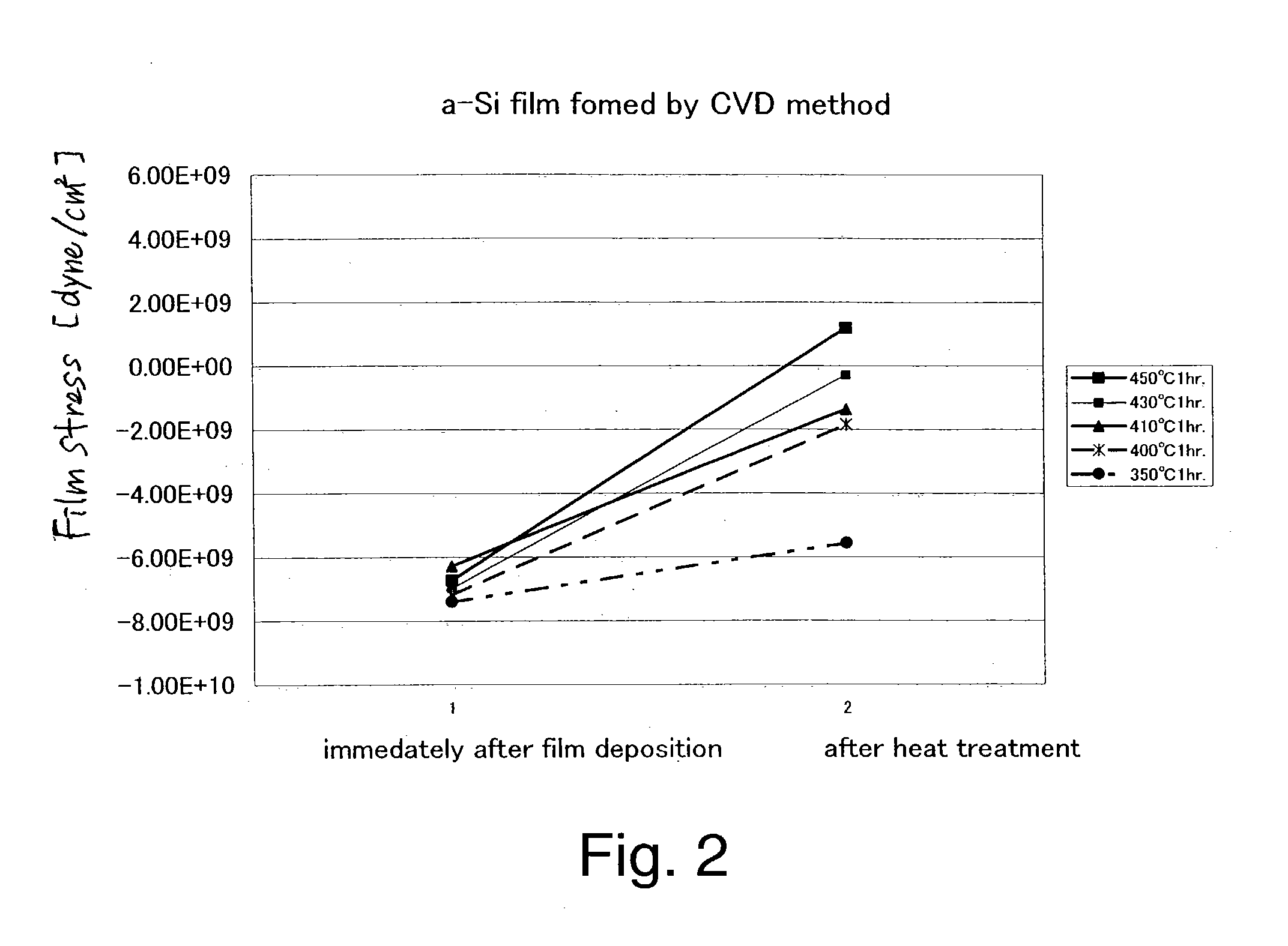
[0084]An amorphous silicon film containing hydrogen was formed on a glass substrate by PCVD (film deposition temperature of 300° C., film deposition gas SiH4), then, heat treatments were performed under various conditions, and the respective stresses were measured. The obtained results are shown in FIG. 2. The respective heat treatment conditions are: 350° C. for one hour; 400° C. for one hour; 410° C. for one hour; 430° C. for one hour; and 450° C. for one hour.

[0085]It is seen from FIG. 2 that the stress value obtained through the heat treatment is changed more toward a tensile stress compared with the stress value obtained immediately after the film deposition (−8×10⁹ (Dyne / cm2) to −6×10⁹ (Dyne / cm2)) under any condition. The stress value obtained after the heat treatment falls in a range of −6×10⁹ (Dyne / cm2) to 2×10⁹ (Dyne / cm2).

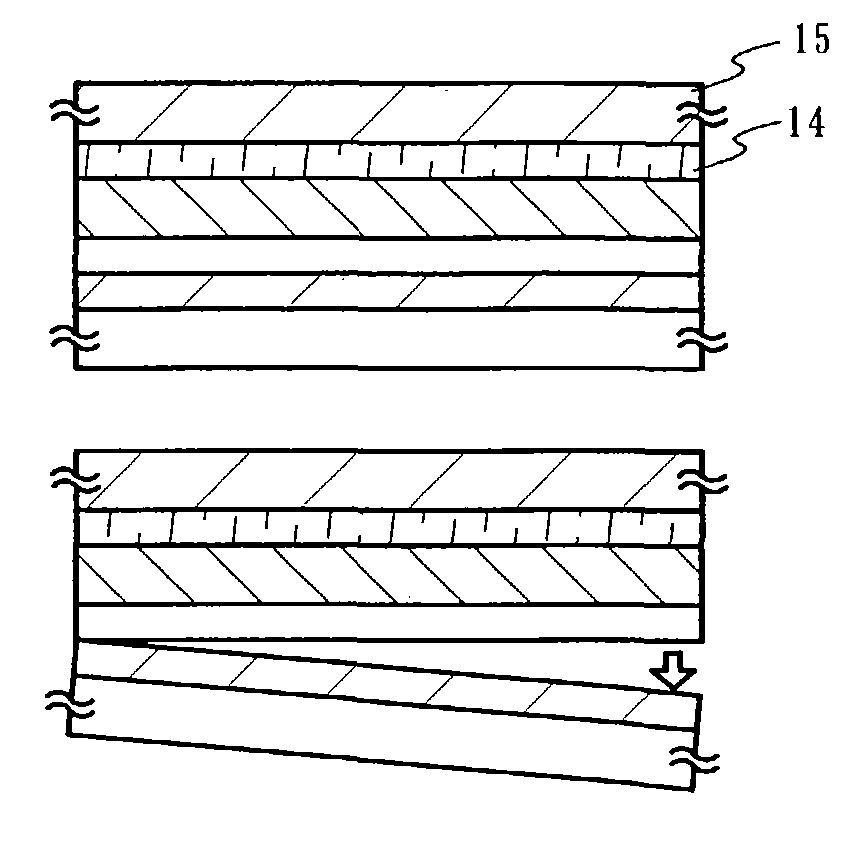
[0086]Further, a tungsten film, a silicon oxide film formed by sputtering, a base insulating film, and an amorphous silicon film containing hydrogen forme...

experiment 2

[0087]As to the amorphous silicon film containing hydrogen obtained by PCVD under the same condition as in Experiment 1, a hydrogen concentration thereof was measured through FT-IR. As a result, Si—H was 1.06×10²² (atoms / cm3), Si—H2 was 8.34×10¹⁹ (atoms / cm3), and the calculated hydrogen concentration in the composition ratio was 21.5%. Further, the hydrogen concentration was similarly calculated under the changed film deposition conditions with PCVD, as a result of which the obtained hydrogen concentrations in the composition ratio were 16.4%, 17.1%, and 19.0%.

[0088]Further, a tungsten film, a silicon oxide film formed by sputtering, a base insulating film, and an amorphous silicon film containing hydrogen formed by PCVD (film with a hydrogen concentration in the composition ratio is 16.4% to 21.5%) were sequentially laminated on a glass substrate. The heat treatment at 410° C. for one hour was performed to each of the resultant lamination layers. Then, a peeling experiment was perf...

experiment 3

[0090]Here, a W film (100 nm) and a silicon oxide film (100 nm) were laminated on a silicon wafer. Then, heat treatments (at 350° C. for one hour, 400° C. for one hour, 410° C. for one hour, 430° C. for one hour, and 450° C. for one hour) were performed thereto. Further, etching was conducted to the silicon oxide film. The results of the measurement of the stress change for the respective treatments are shown in FIG. 3.

[0091]As to the deposition condition of the W film, a tungsten target was used with sputtering, and a film deposition pressure of 0.2 Pa, a film deposition power of 3 kW, and an argon flow rate of 20 sccm were adopted.

[0092]Further, as to the deposition condition of the silicon oxide film: an RF type sputtering device was used; a silicon oxide target (with a diameter of 30.5 cm) was used; an argon gas heated for heating a substrate was flown at a flow rate of 30 sccm; and a substrate temperature of 300° C., a film deposition pressure of 0.4 Pa, a film deposition power...


PUM


Abstract

A peeling method is provided which does not cause damage to a layer to be peeled, and the method enables not only peeling of the layer to be peeled having a small area but also peeling of the entire layer to be peeled having a large area at a high yield. Further, there are provided a semiconductor device, which is reduced in weight through adhesion of the layer to be peeled to various base materials, and a manufacturing method thereof. In particular, there are provided a semiconductor device, which is reduced in weight through adhesion of various elements, typically a TFT, to a flexible film, and a manufacturing method thereof. A metal layer or nitride layer is provided on a substrate; an oxide layer is provided contacting with the metal layer or nitride layer; then, a base insulating film and a layer to be peeled containing hydrogen are formed; and heat treatment for diffusing hydrogen is performed thereto at 410° C. or more. As a result, complete peeling can be attained in the oxide layer or at an interface thereof by using physical means.

Description

BACKGROUND OF THE INVENTION[0001]1. Field of the Invention[0002]The present invention relates to a peeling method of a layer to be peeled, especially, a peeling method of a layer to be peeled containing various elements. In addition to that, the present invention relates to a semiconductor device comprising a circuit composed of a thin film transistor (hereinafter referred to as TFT) transferred by sticking a separated layer to be peeled to a substrate and its manufacturing method. The invention relates, for example, an electrooptical device such as a liquid crystal module, a light emitting device such as an EL module, and an electronic apparatus containing such devices as components therein.[0003]The term semiconductor device, in this specification, covers any device as a whole capable of functioning by utilizing semiconductor characteristics and an electro optical device, a light emitting device, a semiconductor circuit, and electronic apparatuses are all included in the semicondu...

Claims


Application Information

Patent Timeline
Patent Type & Authority Patents(United States)
IPC IPC(8): H01L21/30H01L21/762H01L29/786H01L21/77H01L21/84
CPCH01L21/76251H01L27/1266H01L27/1214H01L27/1218
Inventor TAKAYAMA, TORUMARUYAMA, JUNYAGOTO, YUUGOOHNO, YUMIKOTSURUME, TAKUYAKUWABARA, HIDEAKI
Owner SEMICON ENERGY LAB CO LTD
Why Eureka
Try Eureka